

NTE NTE981 Datasheet

NTE981
Integrated Circuit
Positive 3 Terminal Voltage Regulator, 100mA
Description:
The NTE981 is a positive 3–terminal voltage regulator available in a TO92 type package. With adequate heat sinking this device can deliver 100mA output current. Current limiting is included to limit
peak output current to safe value. Safe area protection for the output transistors is provided to limit
internal power dissipation. If internal power dissipation becomes too high for the heat sinking provided, the thermal shutdown circuit takes over preventing the IC from overheating.
When used as a zener diode/resistor combination replacement, the NTE981 usually results in an effective output impedance improvement of two orders of magnitude, and lower quiescent current.
These regulators can provide local on card regulation, eliminating the distribution problems
associated with single point regulation. T ypical applications include use in logic systems, instrumentation, HiFi, and other solid state electronic equipment. Although designed primarily as fixed voltage
regulator this device can be used with external components to obtain adjustment voltages and currents.
Features:
D Output Voltage Tolerances of ±5% over the Temperature Range
D Output Current of 100mA
D Internal Thermal Overload Protection
D Output Transistor Safe Area Protection
D Internal Short Circuit Current Limit
Absolute Maximum Ratings:
Output Voltage, V
Input Voltage, V
Internal Power Dissipation (Note 1), P
Operating Temperature Range, T
Maximum Junction Temperature, T
Storage Temperature Range, T
OUT
IN
D
opr
J
stg
Lead Temperature (Soldering, 10 sec), T
Internally Limited. . . . . . . . . . . . . . . . . . . . . . . . . . . . . . . . . . .
0°C to +70°C. . . . . . . . . . . . . . . . . . . . . . . . . . . . . . . . . . . . . . . . . .
–55°C to +150°C. . . . . . . . . . . . . . . . . . . . . . . . . . . . . . . . . . . . . . . .
L
8V. . . . . . . . . . . . . . . . . . . . . . . . . . . . . . . . . . . . . . . . . . . . . . . . . . . . . . . . . . . . . . . .
30V. . . . . . . . . . . . . . . . . . . . . . . . . . . . . . . . . . . . . . . . . . . . . . . . . . . . . . . . . . . . . . . . . .
+125°C. . . . . . . . . . . . . . . . . . . . . . . . . . . . . . . . . . . . . . . . . . . . . . .
+260°C. . . . . . . . . . . . . . . . . . . . . . . . . . . . . . . . . . . . . . . . . .
Note 1. Thermal resistance is +180°C/W junction–to–ambient with 0.4” leads from a P.C. board and
+160°C/W junction–to–ambient with 0.125” lead length to a P.C. board.
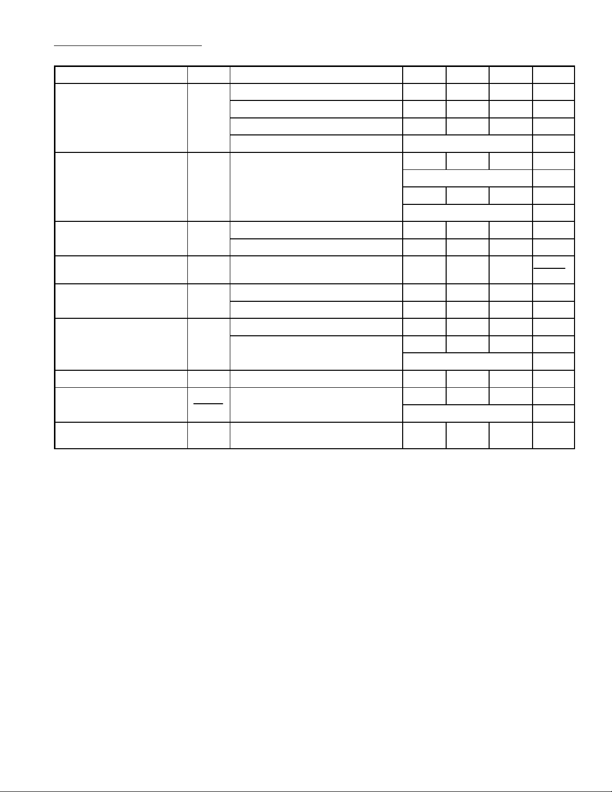
Electrical Characteristics: (TJ = 0° to +125°C, VIN = 14V, IO = 40mA, CIN = 0.33µF, CO = 0.1µF,
Note 2 unless otherwise specified)
Parameter Symbol Test Conditions Min Typ Max
Output Voltage
V
(Note 4)
Line Regulation ∆V
Load Regulation ∆V
Long Term Stability ∆V
Quiescent Current I
Quiescent Current Change
∆I
TJ = +25°C 7.7 8.0 8.3 V
O
1mA ≤ IO ≤ 70mA 7.6 – 8.4 V
1mA ≤ IO ≤ 70mA 7.6 – 8.4 V
V
≤ VIN ≤ V
MIN
TJ = +25°C – 12 85 mV
O
MAX
(7 ≤ VIN ≤ 20)
(1 1 ≤ VIN ≤ 23) V
– 20 100 mV
(10.5 ≤ VIN ≤ 23) V
TJ = +25°C, 1mA ≤ IO ≤ 40mA – 8 40 mV
O
TJ = +25°C, 1mA ≤ IO ≤ 100mA – 25 80 mV
O
TJ = +25°C – 3 5 mA
Q
– 20 –
TJ = +125°C – – 4.7 mA
1mA ≤ IO ≤ 40mA – – 0.1 mA
Q
V
≤ VIN ≤ V
MIN
MAX
– – 1.0 mA
(1 1 ≤ VIN ≤ 23) V
Unit
mV
1000Hrs
Output Noise Voltage V
Ripple Rejection
∆V
∆V
Input Voltage Required to
TJ = +25°C, Note 3, f = 10Hz to 10kHz – 60 – µV
n
f = 120Hz 43 57 – dB
IN
IN
OUT
(12 ≤ VIN ≤ 23) V
TJ = +25°C 10.5 – – V
Maintain Line Regulation
Note 2. The maximum steady state usable output current and input voltage are very dependent on
the heat sinking and/or lead length of the package. The data above represent pulse test
conditions with junction temperatures as indicated at the initiation of test.
Note 3. Recommended minimum load capacitance of 0.01µF to limit high frequency noise band-
width.
Note 4. The temperature coefficient of V
is typically within ±0.01% VO/°C.
OUT
 Loading...