

NTE NTE978, NTE978SM Datasheet

NTE978/NTE978C/NTE978SM
Integrated Circuit
Dual Timer
Description:
The NTE978 series dual timing circuit is a highly stable controller capable of producing accurate time
delays or oscillation. The NTE978 is a dual NTE955. Timing is provided by an external resistor and
capacitor for each timing function. The two timers operate independently of each other sharing only
and GND. The circuits may be triggered and reset on falling waveforms. The output structures
V
CC
may sink or source 200mA.
Features:
D Direct Replacement for 556 Timers
D Replaces Two 555 Timers
D Timing from Microseconds through Hours
D Operates in both Astable and Monostable Modes
D Adjustable Duty Cycle
D Output can Source or Sink 200mA
D Output and Supply TTL Compatible
D Temperature Stability better than 0.005% per °C
D Normally On and Normally Off Output
D Available in Three Types:
NTE978 14–Lead DIP
NTE978C 14–Lead DIP (CMOS)
NTE978SM SOIC–14 (Surface Mount)
Applications:
D Precision Timing
D Pulse Generation
D Sequential Timing
D Time Delay Generation
D Pulse Width Modulation
D Pulse Position Modulation
D Linear Ramp Generator
Absolute Maximum Ratings:
Supply Voltage, V
Power Dissipation (Note 1), P
Operating Temperature Range, T
Storage Temperature Range, T
CC
D
A
stg
Lead Temperature (During Soldering, 10sec Max), T
0° to +70°C. . . . . . . . . . . . . . . . . . . . . . . . . . . . . . . . . . . . . . . . . . . . .
–65° to +150°C. . . . . . . . . . . . . . . . . . . . . . . . . . . . . . . . . . . . . . . . . .
L
+18V. . . . . . . . . . . . . . . . . . . . . . . . . . . . . . . . . . . . . . . . . . . . . . . . . . . . . . . . . . . . . . .
1620mW. . . . . . . . . . . . . . . . . . . . . . . . . . . . . . . . . . . . . . . . . . . . . . . . . .
+260°C. . . . . . . . . . . . . . . . . . . . . . . . . . . . . . . .
Note 1. For operating at elevated temperaturesthe device must be derated based on a +150°C maxi-
mum junction temperature and a thermal resistance of +77°C/W for NTE978 and NTE978C
and +110°C/W for NTE978SM.
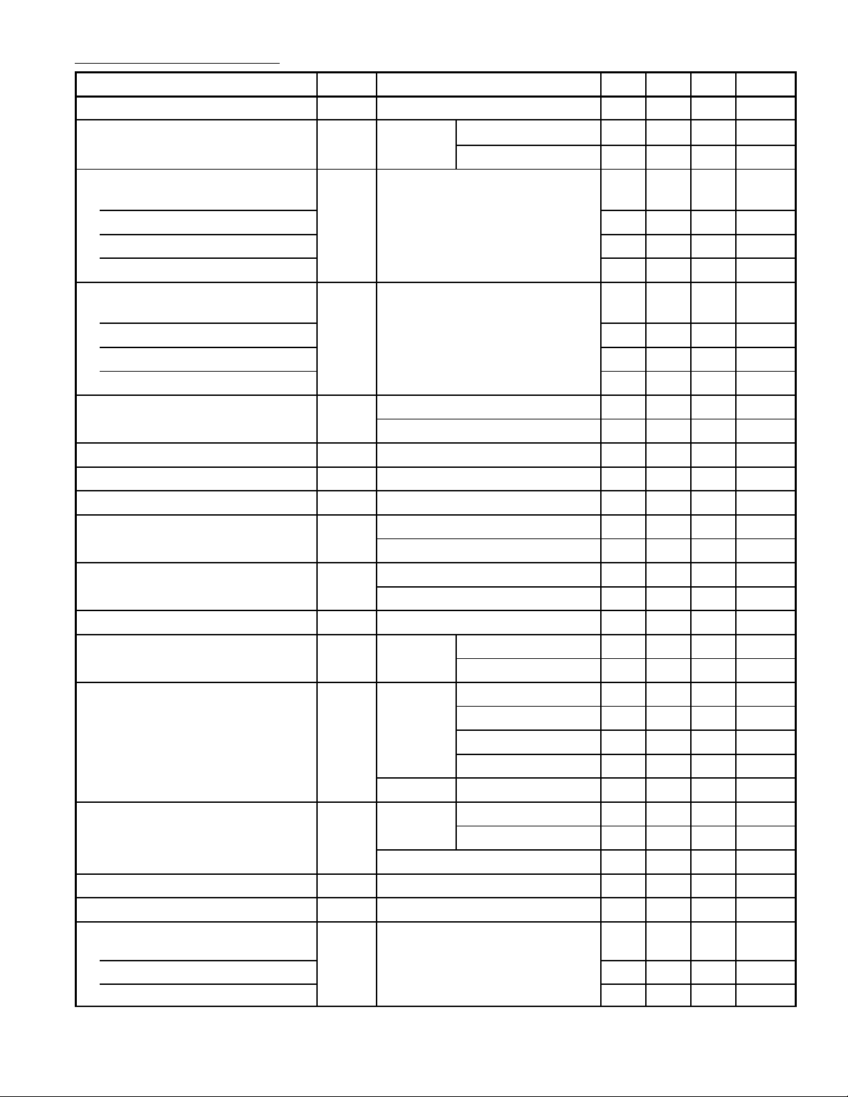
Electrical Characteristics: (TA = +25°C, VCC = +5V to +15V, unless otherwise specified)
Parameter Symbol Test Conditions Min Typ Max Unit
Supply Voltage V
Supply Current (Each Timer Section) I
CC
CC
Low State,
Note 2
VCC = 5V, RL = ∞
VCC = 15V, RL = ∞ – 10 14 mA
4.5 – 16 V
– 3 6 mA
Timing Error, Monostable
Initial Accuracy
Drift with Temperature
Accuracy over Temperature
RA = 1k to 100kΩ, C = 0.1µF,
Note 3
– 0.75 – %
– 50 – ppm/°C
– 1.5 – %
Drift with Supply – 0.1 – %/V
Timing Error, Astable
Initial Accuracy
Drift with Temperature
Accuracy over Temperature
RA, RB = 1k to 100kΩ, C = 0.1µF,
Note 3
– 2.25 – %
– 150 – ppm/°C
– 3.0 – %
Drift with Supply – 0.30 – %/V
Trigger Voltage V
VCC = 15V 4.5 5.0 5.5 V
T
VCC = 5V 1.25 1.67 2.0 V
Trigger Current I
Reset Voltage V
Reset Current I
Threshold Current I
T
Note 4 0.4 0.5 1.0 V
R
R
VTH = V–Control, Note 5 – 0.03 0.1 µA
TH
– 0.2 1.0 µA
– 0.1 0.6 mA
VTH = 11.2V – – 250 nA
Control Voltage Level and V
Threshold Voltage
Pin1, Pin13 Leakage Output High I
V
VCC = 15V 9 10 11 V
CL
TH
VCC = 5V 2.6 3.33 4.0 V
dis
– 1 100 nA
Pin1, Pin13 Saturation Output Low Note 6 VCC = 15V, I = 15mA – 180 300 mV
VCC = 4.5V, I = 4.5mA – 80 200 mV
Output Voltage Drop (Low) V
Output Voltage Drop (High) V
OL
OH
VCC = 15V I
VCC = 5V I
VCC = 15V I
= 10mA – 0.1 0.25 V
SINK
I
= 50mA – 0.4 0.75 V
SINK
I
= 100mA – 2.0 2.75 V
SINK
I
= 200mA – 2.5 – V
SINK
= 5mA – 0.25 0.35 V
SINK
SOURCE
I
SOURCE
= 200mA – 12.5 – V
= 100mA 12.75 13.3 – V
VCC = 5V 2.75 3.3 – V
Rise Time of Output t
Fall Time of Output t
OLH
OHL
– 100 – ns
– 100 – ns
Matching Characteristics
Initial Timing Accuracy
Timing Druft with Temperature
Note 7
– 0.1 2.0 %
– ±10 – ppm/°C
Drift with Supply Voltage – 0.2 0.5 %/V
 Loading...