

NTE NTE975SM Datasheet

NTE975 & NTE975SM
Integrated Circuit
Operational Amplifier
Description:
The NTE975 and NTE975SM are general purpose operational amplifiers built on a single chip. The
resulting close match and tight thermal coupling gives low offsets and temperature drift as well as fast
recovery from thermal transients.
The unity–gain compensation specified makes the circuit stable for all feedback configurations, even
with capacitive loads. However, it is possible to optimize compensation for the best high frequency
performance at any gain. As a comparator, the output can be clamped at any desired level to make
it compatible with logic circuits.
Features:
D Available in 8–Lead Mini DIP (NTE975) and Surface Mount, SOIC–8 (NTE975SM)
D Frequency Compensation with a Single 30pF Capacitor
D Operation From ±5V to ±20V
D Low Current Drain: 1.8mA @ ±20V
D Continuous Short–Circuit Protection
D Operation as a Comparator with Differential Inputs as High as ±30V
D No Latch–Up when Common Mode Range is Exceeded
Absolute Maximum Ratings:
Supply Voltage, V
Power Dissipation (Note 1), P
Differential Input Voltage, V
Input Voltage (Note 2), V
Output Short–Circuit Duration (Note 3), t
Operating Temperature Range, T
Storage Temperature Range, T
S
D
ID
IN
s
A
stg
Lead Temperature (During Soldering, 10sec), T
0° to +70°C. . . . . . . . . . . . . . . . . . . . . . . . . . . . . . . . . . . . . . . . . . . . .
–65° to +150°C. . . . . . . . . . . . . . . . . . . . . . . . . . . . . . . . . . . . . . . . . .
L
±22V. . . . . . . . . . . . . . . . . . . . . . . . . . . . . . . . . . . . . . . . . . . . . . . . . . . . . . . . . . . . . . . .
500mW. . . . . . . . . . . . . . . . . . . . . . . . . . . . . . . . . . . . . . . . . . . . . . . . . . .
±30V. . . . . . . . . . . . . . . . . . . . . . . . . . . . . . . . . . . . . . . . . . . . . . . . . . . . . . .
±15V. . . . . . . . . . . . . . . . . . . . . . . . . . . . . . . . . . . . . . . . . . . . . . . . . . . . . . . . .
Indefinite. . . . . . . . . . . . . . . . . . . . . . . . . . . . . . . . . . . . . . . .
+300°C. . . . . . . . . . . . . . . . . . . . . . . . . . . . . . . . . . . .
Note 1. For operating at elevated temperatures the devices must be derated based on a maximum
junction to case thermal resistance of +45°C/W, or +150°C/W junction to ambient.
Note 2. For s upply v oltages l ess t han ±15V, t he a bsolute m aximum input voltage i s e qual t o t he s upply
voltage.
Note 3. Continuous short circuit is allow for ambient temperatures to +70°C.
Electrical Characteristics: (0° ≤ TA ≤ +70°C, ±5V ≤ VS ≤ ±15V unless otherwise specified)
Parameter Symbol Test Conditions Min Typ Max Unit
Input Offset Voltage V
Input Offset Current I
Input Bias Current I
Input Resistance r
Supply Current I
Large Signal Voltage Gain A
Average Temperature Coefficient
of Input Offset Voltage
Output Voltage Swing V
TCV
IO
IO
IB
i
D
v
IORS
O
TA = +25°C, RS ≤ 10kΩ – 1.0 5.0 mV
RS ≤ 10kΩ – – 6.0 mV
TA = +25°C – 40 200 nA
– – 300 nA
TA = +25°C – 120 500 nA
– – 0.8 µA
TA = +25°C 300 800 – kΩ
TA = +25°C, VS = ±15V – 1.8 2.8 mA
TA = +125°C, VS = ±15V – 1.2 2.25 mA
TA = +25°C, VS = ±15V,
= ±10V, RL ≥ 2kΩ
V
OUT
VS = ±15V, V
≥ 2kΩ
R
L
≤ 50Ω – 3.0 – µV/°C
RS ≤ 10kΩ – 6.0 – µV/°C
VS = ±15V, RL = 10Ω ±12 ±14 – V
VS = ±15V, RL = 2kΩ ±10 ±13 – V
OUT
= ±10V,
50 160 – V/mV
25 – – V/mV
Input Voltage Range V
Common Mode Rejection Ratio CMRR RS ≤ 10kΩ 70 90 – dB
Supply Voltage Rejection Ratio PSRR RS ≤ 10kΩ 77 90 – dB
Compensation
Inverting Input
Non–Inverting Input
V (–)
ICR
1
2
3
4
VS = ±15V ±12 – – V
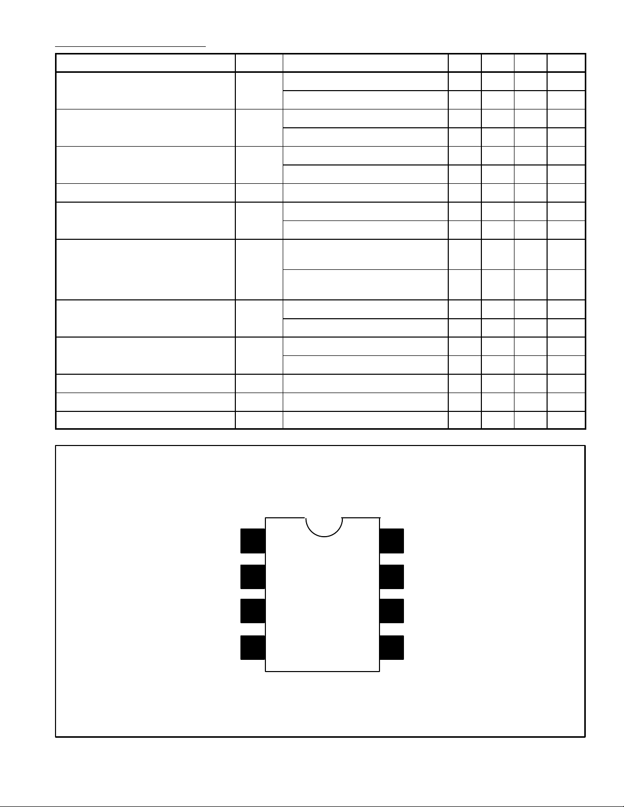
Pin Connection Diagram
Compensation
8
7
V (+)
6
Output
5 Balance
 Loading...