

NTE973D
Integrated Circuit
Double Balanced Modulator/Demodulator
Description:
The NTE973D is a balanced modulatior/demodulator in a 14–Lead DIP type package designed for
use where the output voltage is a product of an input voltage (signal) and a switching function (carrier).
Typical applications include suppressed carrier and amplitude modulation, synchronous detection,
FM detection, phase detection, and chopper applications.
Features:
D Excellent Carrier Suppression:
65dB typ @ 0.5MHz
50db typ @ 10MHz
D Adjustable Gain and Signal Handling
D Balanced Inputs and Outputs
Absolute Maximum Ratings:
(TA = +25°C unless otherwise specified)
Applied Voltage, ∆V
(V
Differential Input Signal, V7–V
Differential Input Signal, V
Maximum Bias Current, I
Operating Temperature Range, T
Storage Temperature Range, T
, V8–V1, V9–V7, V9–V8, V7–V4, V7–V1, V8–V4, V6–V8, V2–V5, V3–V5) 30V. . . . . . . . .
6–V7
8
4–V1
5
A
stg
Thermal Resistance, Junction–to–Ambient, R
Electrical Characteristics:
(VCC = 12V, VEE = –8V, I5 = 1mA, RL = 3.9kΩ, Re = 1kΩ, TA = +25°C,
Note 1 unless otherwise specified)
Parameter Symbol Test Conditions Min Typ Max Unit
Carrier Feedthrough V
Carrier Suppression V
CFT
VC = 60mV
and offset adjusted to
zero
VC = 300mV
wave, fC = 1kHz
fS = 10kHz, 300mV
CS
60mV
rms
thJA
sine wave
rms
P–P
sine wave
square
rms
±(5 + I5Re) V. . . . . . . . . . . . . . . . . . . . . . . . . . . . . . . . . . . . . . . . . . . . . . .
–65° to +150°C. . . . . . . . . . . . . . . . . . . . . . . . . . . . . . . . . . . . . . . . . .
fC = 1kHz – 40 – µV
fC = 10MHz – 140 – µV
Offset adjusted to zero – 0.04 0.4 mV
Offset not adjusted – 20 200 mV
fC = 500kHz 40 65 – dB
,
fC = 10MHz – 50k – dB
+5.0V. . . . . . . . . . . . . . . . . . . . . . . . . . . . . . . . . . . . . . . . . . . . . . . . . . . . .
10mA. . . . . . . . . . . . . . . . . . . . . . . . . . . . . . . . . . . . . . . . . . . . . . . . . . . . . . . . .
0° to +70°C. . . . . . . . . . . . . . . . . . . . . . . . . . . . . . . . . . . . . . . . . . . . .
100°C/W. . . . . . . . . . . . . . . . . . . . . . . . . . . . . . . . . .
rms
rms
rms
rms
Note 1. All input and output characteristics are single–ended unless otherwise specified)
Electrical Characteristics (Cont’d): (VCC = 12V, VEE = –8V, I5 = 1mA, RL = 3.9kΩ, Re = 1kΩ,
T
= +25°C, Note 1 unless otherwise specified)
A
Parameter Symbol Test Conditions Min Typ Max Unit
Transadmittance Bandwidth (Magnitude) BW
Signal Gain A
|I
|TC
|TC
r
c
r
c
bS
I
bC
ioS
ioC
CC
I
EE
Single–Ended Input Impedance,
Signal Port
Single–Ended Output Impedance,
Signal Port
Input Bias Current I
Input Offset Current |I
Average Temperature Coefficient of
Input Offset Current
Output Offset Current |Ioo| I6 – I
Average Temperature Coefficient of
Output Offset Current
Common–Mode Input Swing CMV Signal Port, fS = 1kHz – 5.0 – V
Common–Mode Gain ACM Signal Port, fS = 1kHz, |VC| = 0.5V – –85 – dB
Common–Mode Quiescent Output Voltage V
Differential Output Voltage Swing Capability V
Power Supply Current I
DC Power Dissipation P
Carrier Input Port, RL = 50Ω, VC = 60mV
3dB
wave, f
= 1kHz, 300mV
S
Signal Input Port, RL = 50Ω, VS = 300mV
wave, |V
VS = 100mV
VS
Parallel Input Resistance, f = 5MHz – 200 – kΩ
ip
Parallel Input Capacitance, f = 5MHz – 2.0 – pF
ip
Parallel Output Resistance, f = 10MHz – 40 – kΩ
op
Parallel Output Capacitance, f = 10MHz – 5.0 – pF
op
IbS = (I1 + I4) / 2 – 12 30 µA
IbC = (I7 + I8) / 2 – 12 30 µA
| I
ioS
| IioC = I7 – I
| TA = –55° to +125°C – 2.0 – nA/°C
Iio
| TA = –55° to +125°C – 90 – nA/°C
Ioo
Pin6 or Pin9 – 8.0 – V
out
out
I6 + I
I
10
D
= I1 – I
9
9
| = 0.5V
C
, f = 1kHz, |VC| = 0.5V 2.5 3.5 – V/V
rms
4
8
sine wave
rms
rms
rms
sine
sine
– 300 – MHz
– 80 – MHz
– 0.7 7.0 µA
– 0.7 7.0 µA
– 14 80 µA
– 8.0 – V
– 2.0 4.0 mA
– 3.0 5.0 mA
– 33 – mW
P–P
P–P
P–P
Note 1. All input and output characteristics are single–ended unless otherwise specified)
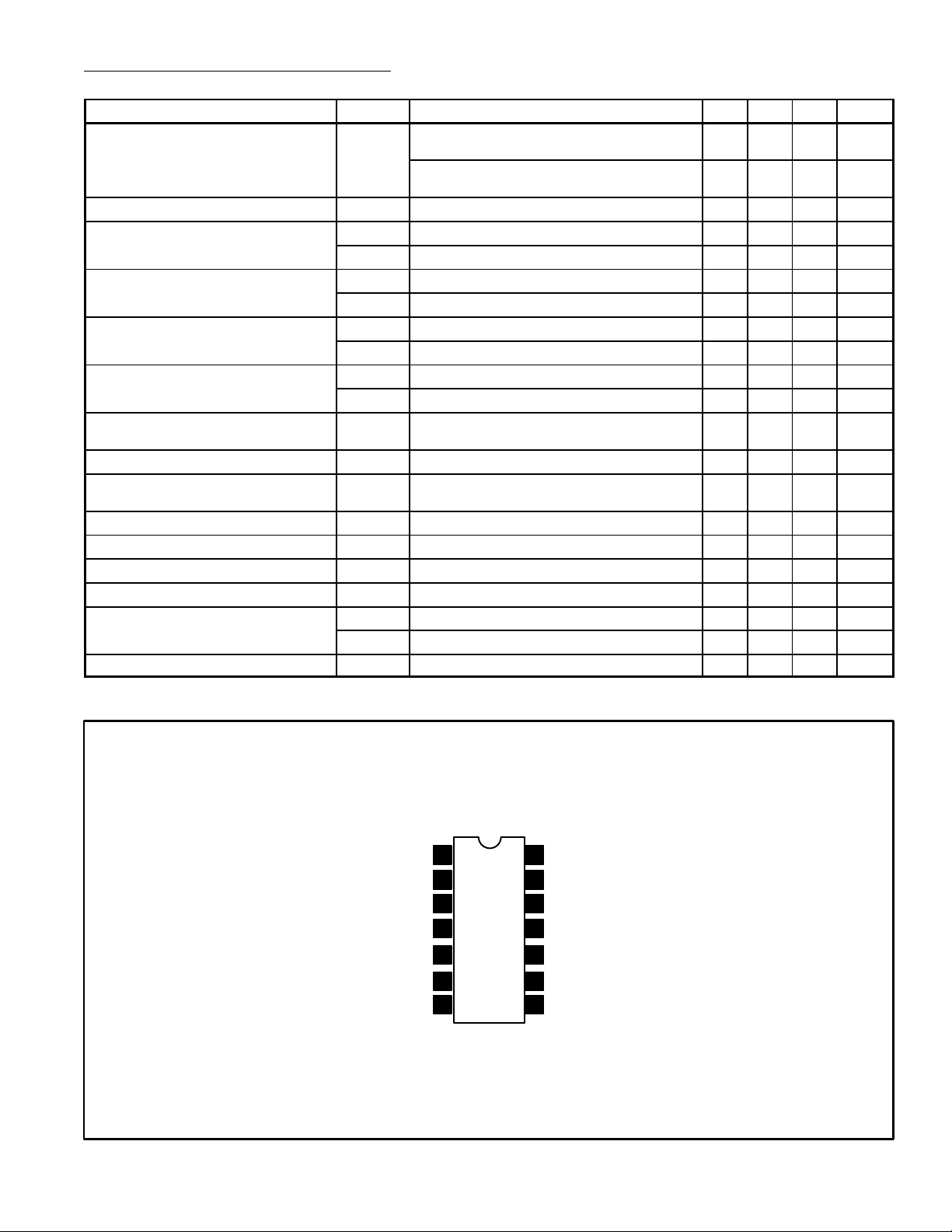
Pin Connection Diagram
(+) Signal Input
Gain Adjust
Gain Adjust
(–) Signal Input
Bias
(+) Output
N.C.
1
2
3
4
5
6
7
V (–)
14
N.C.
13
(–) Output
12
N.C.
11
(–) Carrier Input
10
N.C.
9
(+) Carrier Input
8
 Loading...