

NTE NTE967 Datasheet
NTE967
Linear Integrated Circuit
Voltage Regulator, Negative, –12V, 1A
Description:
The NTE967 is a negative voltage regulator in a TO220 type package that employs current limiting,
thermal shutdown, and safe–area compensation which makes it remarkably rugged under most operating conditions. With adequate heat–sinking they can deliver output currents in excess of 1.0 amperes.
Features:
D Thermal Short Circuit and safe Area Protection
D High Ripple Rejection
Absolute Maximum Ratings:
Input Voltage, V
IN
Input–Output Differential 30V. . . . . . . . . . . . . . . . . . . . . . . . . . . . . . . . . . . . . . . . . . . . . . . . . . . . . . . . . . . .
Power Dissipation (Note 1), P
Operating Junction Temperature Range, T
Storage Temperature Range, T
D
J
stg
Lead Temperature (During Soldering, 10sec), T
L
Internally Limited. . . . . . . . . . . . . . . . . . . . . . . . . . . . . . . . . . . . . . . . . . .
0° to +125°C. . . . . . . . . . . . . . . . . . . . . . . . . . . . . . . . . . . .
–65° to +150°C. . . . . . . . . . . . . . . . . . . . . . . . . . . . . . . . . . . . . . . . . .
–40V. . . . . . . . . . . . . . . . . . . . . . . . . . . . . . . . . . . . . . . . . . . . . . . . . . . . . . . . . . . . . . . . .
+230°C. . . . . . . . . . . . . . . . . . . . . . . . . . . . . . . . . . . .
Note 1. For calculations of junction temperature rise due to power dissipation, thermal resistance
junction–to–ambient (R
Electrical Characteristics:
(IO = 500mA, CIN = 2.2µF, C
) is 50°C/W (no heat sink) and 5°C/W (infinite heat sink).
thJA
= 1µF, PD = 1.5W, TJ = 0° to +125°C
OUT
unless otherwise specified)
Parameter Symbol Test Conditions Min Typ Max Unit
Output Voltage V
Line Regulation Reg
Load Regulation Reg
O
LoadTJ
TJ = +25°C –11.5 –12.0 –12.5 V
5mA ≤ IO ≤ 1A, PO ≤ 15W,
Line
–27V ≤ V
TJ = +25°C,
Note 2
= +25°C,
Note 2
IN
≤ –14.5V
–30V ≤ VIN ≤ –14.5V – 5 80
–22V ≤ VIN ≤ –16V – 3 30
5mA ≤ IO ≤ 1.5A – 15 200
250mA ≤ IO ≤ 750mA – 5 75 mV
–11.4 –12.0 –12.6 V
mV
mV
Electrical Characteristics: (IO = 500mA, CIN = 2.2µF, C
unless otherwise specified)
Parameter Symbol Test Conditions Min Typ Max Unit
= 1µF, PD = 1.5W, TJ = 0° to +125°C
OUT
Quiescent Current I
Quiescent Current Change ∆I
B
TJ = +25°C – 1.5 3.0 mA
–30V ≤ VIN ≤ –14.5V – – 0.5 mA
B
5mA ≤ IO ≤ 1A – – 0.5
Ripple Rejection RR –25V ≤ VIN ≤ –15V, f = 120Hz 54 70 – dB
Dropout Voltage VIN – VOTJ = +25°C, IO = 1A – 1.1 – V
Output Noise Voltage V
Peak Output Current I
Average Temperature
TCV
max
TA = +25°C, 10Hz ≤ f ≤ 100kHz – 300 – µV/V
n
TJ = +25°C – 2.2 – A
IO = 5mA, 0° ≤ TJ ≤ +100°C – –0.8 – mV/°C
O
O
Coefficient of Output
Voltage
Note 2. Regulation is measured at a contant junction temperature by pulse teting with a low duty
cycle. Changes in output voltage due to heating effects must be taken into account.
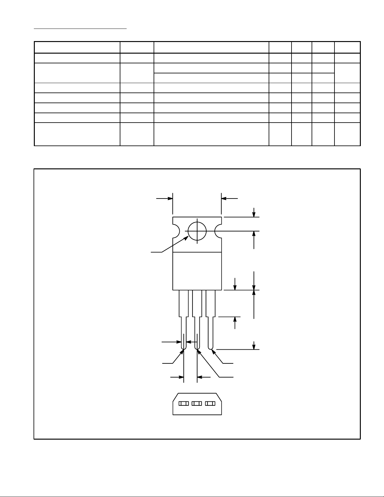
.420 (10.67)
Max
.110 (2.79)
.147 (3.75)
Dia Max
.070 (1.78)
Max
.100 (2.54)
GND
(12.7)
.250 (6.35)
Max
(12.7)
V
OUT
V
/Tab
IN
.500
Max
.500
Min
 Loading...