

NTE NTE963 Datasheet
NTE963
Linear Integrated Circuit
Voltage Regulator, Negative, –6V, 1A
Description:
The NTE963 voltage regulator employs current limiting, thermal shutdown, and safe–area compensation which makes it remarkably rugged under most operating conditions. With adequate heat–
sinking they can deliver output currents in excess of 1.0 amperes.
Features:
D No External Components Required
D Internal Thermal Overload Protection
D Internal Short–Circuit Current Limiting
D Output Transistor Safe–Area Compensation
Absolute Maximum Ratings:
Input Voltage, V
IN
Internal Power Dissipation, P
(TA = +25°C unless otherwise specified)
D
Derate Above +25°C 15.4mW/°C. . . . . . . . . . . . . . . . . . . . . . . . . . . . . . . . . . . . . . . . . . . . . . . . . . .
Thermal Resistance, Junction–to–Ambient, R
Internal Power Dissipation (T
= +25°C), P
C
D
Derate Above +75°C 200mW/°C. . . . . . . . . . . . . . . . . . . . . . . . . . . . . . . . . . . . . . . . . . . . . . . . . . . .
Thermal Resistance, Junction–to–Ambient (T
Maximum Junction Temperature Range, T
Storage Temperature Range, T
Electrical Characteristics:
Parameter Symbol Test Conditions Min Typ Max Unit
Output Voltage V
Line Regulation Reg
stg
(VIN = –11V, IO = 500mA, 0°C ≤ TJ ≤ +125°C unless otherwise specified)
O
LineTJ
J
TJ = +25°C –5.75 –6.0 –6.25 V
5mA ≤ IO ≤ 1A, PO ≤ 15W,
–8.0V ≤ V
= +25°C
thJA
= +25°C), R
C
≤ –21V
IN
–8.0V ≤ VIN ≤ –25V – 43 120
–9.0V ≤ VIN ≤ –13V – 10 60
thJA
–5.7 – –6.3 V
–35V. . . . . . . . . . . . . . . . . . . . . . . . . . . . . . . . . . . . . . . . . . . . . . . . . . . . . . . . . . . . . . . . .
Internally Limited. . . . . . . . . . . . . . . . . . . . . . . . . . . . . . . . . . . . . . . . . . .
65°C/W. . . . . . . . . . . . . . . . . . . . . . . . . . . . . . . . . . .
Internally Limited. . . . . . . . . . . . . . . . . . . . . . . . . . . . . . .
5°C/W. . . . . . . . . . . . . . . . . . . . . . . .
0° to +150°C. . . . . . . . . . . . . . . . . . . . . . . . . . . . . . . . . . . .
–65° to +150°C. . . . . . . . . . . . . . . . . . . . . . . . . . . . . . . . . . . . . . . . . .
mV
Electrical Characteristics: (VIN = –11V, IO = 500mA, 0°C ≤ TJ ≤ +125°C unless otherwise specified)
Parameter Symbol Test Conditions Min Typ Max Unit
Load Regulation Reg
LoadTJ
= +25°C
5mA ≤ IO ≤ 1.5A – 13 120
mV
250mA ≤ IO ≤ 750mA – 5.0 60
Quiescent Current I
Quiescent Current Change ∆I
B
TJ = +25°C – 4.3 8.0 mA
–8.0V ≤ VIN ≤ –25V – – 1.3 mA
B
5mA ≤ IO ≤ 1A – – 0.5
Ripple Rejection RR 9.0V ≤ VIN ≤ 19.0V, f = 120Hz – 65 – dB
Dropout Voltage VIN – VOTJ = +25°C, IO = 1A – 2.0 – V
Output Noise Voltage V
Output Resistance r
Short–Circuit Current Limit I
Peak Output Current I
Average Temperature
TCV
O
sc
max
TA = +25°C, 10Hz ≤ f ≤ 100kHz – 45 – µV/V
n
f = 1kHz – 17 – mΩ
TA = +25°C, VIN = 35V – 0.2 – A
TJ = +25°C – 2.2 – A
O
– –1.0 – mV/°C
Coefficient of Output
Voltage
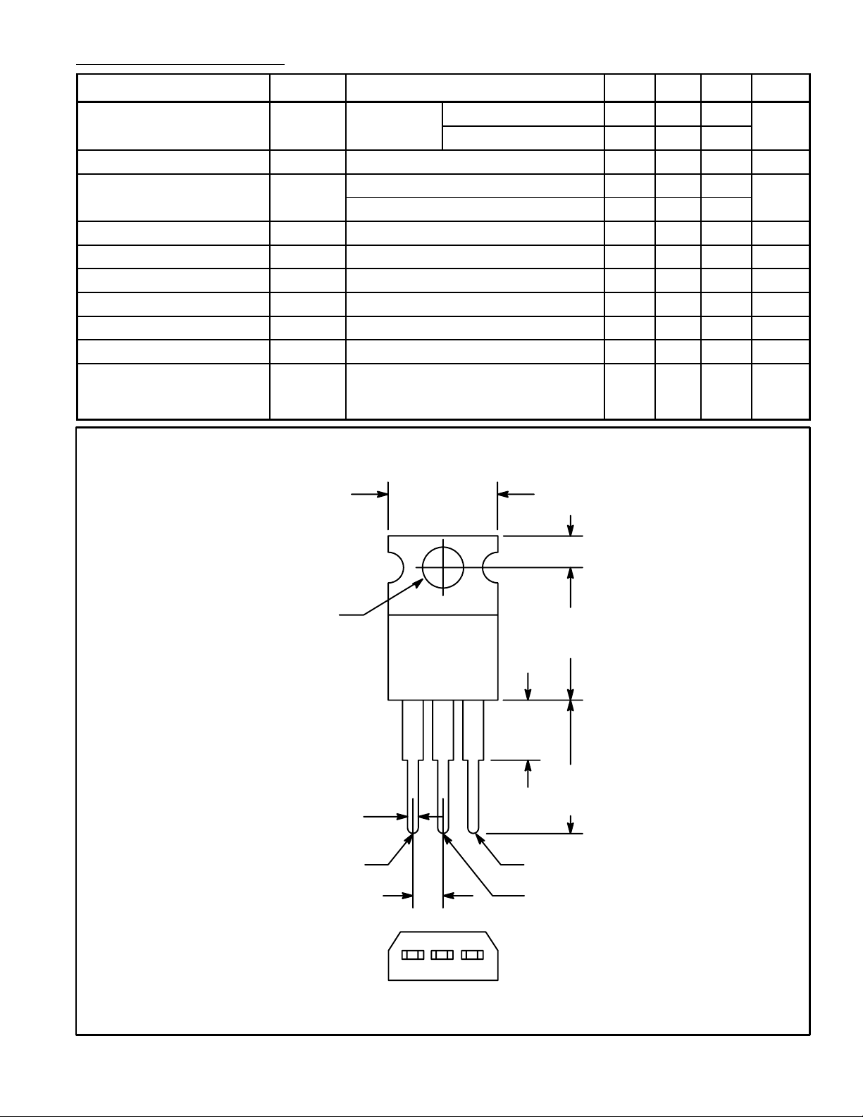
.420 (10.67)
Max
O
.147 (3.75)
Dia Max
.070 (1.78)
Max
.100 (2.54)
GND
.110 (2.79)
(12.7)
.250 (6.35)
Max
(12.7)
V
OUT
V
/Tab
IN
.500
Max
.500
Min
 Loading...