

NTE NTE957 Datasheet

NTE957
Integrated Circuit
3–Terminal Adjustable Negative
Voltage Regulator
Description:
The NTE957 is an adjustable 3–terminal negative voltage regulator in a TO220 type package capable
of supplying i n e xcess o f – 1.5A o ver a – 1.2V t o – 37V o utput r ange. The circuit d esign h as b een optimized
for excellent regulation a nd l ow t hermal t ransients. F urther, the NTE957 f eatures i nternal c urrent limiting,
thermal shutdown, and safe–area compensation, making this device virtually blowout–proof against
overloads.
The NTE957 serves a wide variety of applications including local on–card regulation, programmable–
output voltage regulation or precision current regulation. The NTE957 is the ideal complement to the
NTE956 adjustable positive regulator.
Features:
D Output Voltage Adjustable from –1.2V to –37V
D Guaranteed 1.5A Output Current
D Line Regulation Typically 0.01%/V
D Load Regulation Typically 0.3%
D Excellent Thermal Regulation: 0.002%/W
D 77dB Ripple Rejection
D Temperature–Independent Current Limit
D Internal Thermal Overload Protection
D 100% Electrical Burn–In
D Eliminates the Need to Stock Many Voltages
Absolute Maximum Ratings:
Power Dissipation, P
Input–Output Voltage Differential, V
Operating Junction Temperature Range, T
Storage Temperature Range, T
Typical Thermal Resistance, Junction–to–Case, R
Lead Temperature (During Soldering, 10sec), T
D
I–VO
J
stg
L
thJC
Internally Limited. . . . . . . . . . . . . . . . . . . . . . . . . . . . . . . . . . . . . . . . . . . . . . . . . .
40V. . . . . . . . . . . . . . . . . . . . . . . . . . . . . . . . . . . . . . . . . . . . . . .
0° to +125°C. . . . . . . . . . . . . . . . . . . . . . . . . . . . . . . . . . . .
–65° to +150°C. . . . . . . . . . . . . . . . . . . . . . . . . . . . . . . . . . . . . . . . . .
4°C/W. . . . . . . . . . . . . . . . . . . . . . . . . . . . . . . .
+300°C. . . . . . . . . . . . . . . . . . . . . . . . . . . . . . . . . . . .
Electrical Characteristics: (0° ≤ TJ ≤ +125°C, VIN–V
= 5V, IO = 500mA, I
OUT
= 1.5A, Note 1
MAX
unless otherwise specified)
Parameter Symbol Test Conditions Min Typ Max Unit
Line Regulation Reg
Load Regulation Reg
lineTA
load
Thermal Regulation TA = +25°C, 20ms Pulse – 0.003 0.04 %/W
Adjustment Pin Current I
Adjustment Pin Current
∆I
Adj
Adj
Change
Reference Voltage V
Temperature Stability T
Minimum Load Current I
Maximum Output Current I
ref
S
Lmin
max
Limit
RMS Output Noise,
% of V
OUT
N TA = +25°C, 10Hz ≤ f ≤ 10kHz – 0.003 – %
Ripple Rejection Ratio RR V
Long Term Stability S TA = +125°C, 1000 Hours – 0.3 1.0 %
= +25°C, 3V ≤ (VIN–V
3V ≤ (VIN–V
) ≤ 40V – 0.02 0.07 %/V
OUT
TA = +25°C, 10mA ≤ IO ≤ I
Note 2
10mA ≤ IO ≤ 1
MAX
, Note 2
) ≤ 40V, Note 2 – 0.01 0.04 %/V
OUT
V
MAX
,
≤ 5V – 15 50 mV
OUT
V
≥ 5V – 0.3 1.0 %
OUT
V
≤ 5V – 20 70 mV
OUT
V
≥ 5V – 0.3 1.5 %
OUT
– 65 100 µA
10mA ≤ IL ≤ I
= +25°C
T
A
, 2.5V ≤ (VIN–V
MAX
OUT
) ≤ 40V,
– 2 5 µA
TA = +25°C –1.213 –1.250 –1.287 V
3V ≤ (VIN–V
P ≤ P
MAX
) ≤ 40V, 10mA ≤ IO ≤ 1
OUT
MAX
,
–1.200 –1.250 –1.300 V
0° ≤ TJ ≤ +125°C – 0.6 – %
(VIN–V
(VIN–V
VIN–V
VIN–V
OUT
) ≤ 40V – 2.5 10 mA
OUT
) ≤ 10V – 1.5 6.0 mA
OUT
≤ 15V 1.5 2.2 – A
OUT
= 40V – 0.4 – A
OUT
= 10V, f = 120Hz – 60 – dB
C
= 10µF 66 77 – dB
ADJ
Note 1. Although power dissipation is internally limited, these specifications are applicable for power
dissipations of 20W.
Note 2. Regulation is measured at constant junction temperature, using pulse testing with a low duty
cycle. Changes in output voltage due to heating effects are covered under the specification
for thermal regulation.
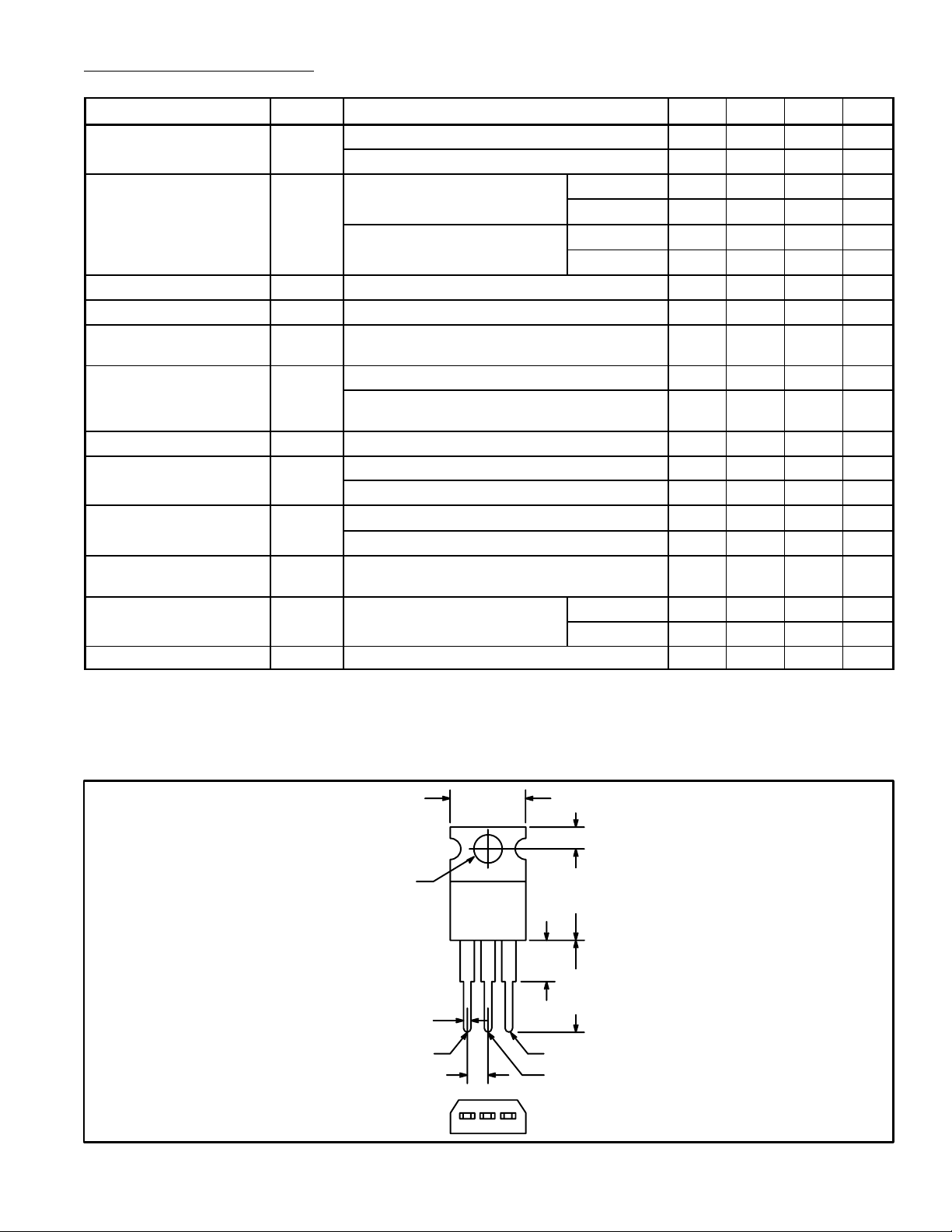
.420 (10.67)
Max
.110 (2.79)
.250
(6.35)
Max
.500
(12.7)
Max
.500
(12.7)
V
OUT
V
IN
Min
/Tab
.147 (3.75)
Dia Max
.070 (1.78)
Max
Adj
.100 (2.54)
 Loading...