

NTE NTE955S, NTE955M, NTE955SM Datasheet

NTE955M
NTE955S
NTE955SM
Integrated Circuit
Timing Circuit
Description:
The NTE955 series timing circuit is a highly stable controller capable of producing accurate time delays, or oscillation. Additional terminals are provided for triggering or resetting if desired. In time delay
mode of operation, the time is precisely controlled by one external resistor and capacitor. For astable
operation as an oscillator, the free running frequency and the duty cycle are both accurately controlled
with two external resistors and one capacitor. The circuit may be triggered and reset on falling waveforms, and the output structure can source or sink up to 200mA or drive TTL circuits.
Features:
D Direct Replacement for 555 Timers
D Timing from Microseconds through Hours
D Operates in Both Astable and Monostable Modes
D Adjustable Duty Cycle
D High Current Output Can Source or Sink 200mA
D Output and Supply TTL Compatible TTL
D Temperature Stability of 0.005% per °C
D Normally “ON” or Normally “OFF” Output
D Available in Three Types:
NTE955M – 8–Lead DIP
NTE955S – 8–Lead SIP
NTE955SM – SOIC–8 (Surface Mount)
Applications:
D Precision Timing
D Pulse Generation
D Sequential Timing
D Time Delay Generation
D Pulse Width Modulation
D Pulse Position Modulation
D Linear Ramp Generator
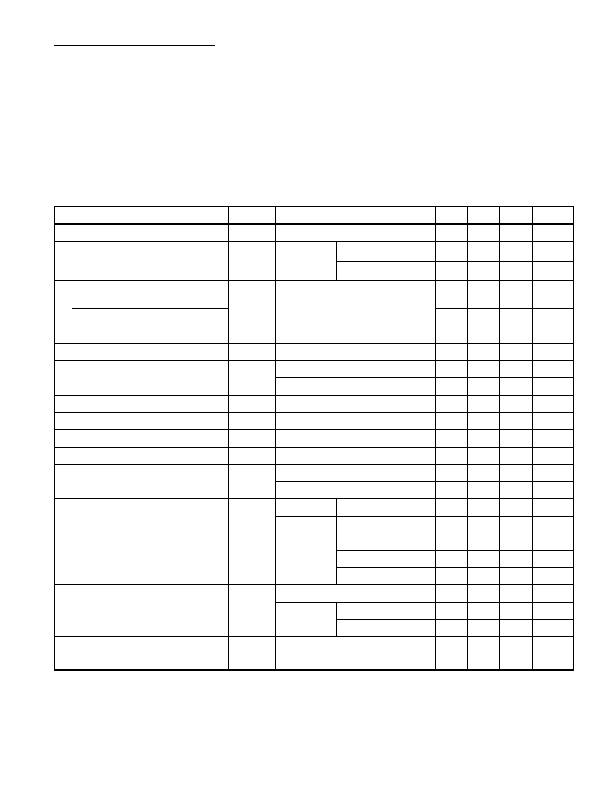
Absolute Maximum Ratings: (TA = +25°C unless otherwise specified)
Power Supply Voltage. V
Discharge Current (Pin7), I
Power Dissipation, P
CC
7
D
Derate Above 25°C 5mW/°C. . . . . . . . . . . . . . . . . . . . . . . . . . . . . . . . . . . . . . . . . . . . . . . . . . . . . . .
Operating Temperature Range, T
Storage Temperature Range, T
Lead Temperature (During Soldering, 10sec), T
stg
A
–65° to +150°C. . . . . . . . . . . . . . . . . . . . . . . . . . . . . . . . . . . . . . . . . .
L
Electrical Characteristics: (TA = +25°C, VCC = 5V to 15V unless otherwise specified)
Parameter Symbol Test Conditions Min Typ Max Unit
18V. . . . . . . . . . . . . . . . . . . . . . . . . . . . . . . . . . . . . . . . . . . . . . . . . . . . . . . . . .
200mA. . . . . . . . . . . . . . . . . . . . . . . . . . . . . . . . . . . . . . . . . . . . . . . . . . . . . .
625mW. . . . . . . . . . . . . . . . . . . . . . . . . . . . . . . . . . . . . . . . . . . . . . . . . . . . . . . . . .
0° to +70°C. . . . . . . . . . . . . . . . . . . . . . . . . . . . . . . . . . . . . . . . . . . . .
+260°C. . . . . . . . . . . . . . . . . . . . . . . . . . . . . . . . . . . .
Operating Supply Voltage Range V
Supply Current I
CC
CC
RL = ∞,
VCC = 5V – 3.0 6.0 mA
4.5 – 16 V
Low State,
VCC = 15V – 10 15 mA
– 1.0 – %
Timing Error
Initial Accuracy C = 0.1µF
Note 2
R = 1kΩ to 100kΩ, Note 3
Drift with Temperature – 50 – ppm/°C
Drift with Supply Voltage – 0.1 – %/V
Threshold Voltage V
Trigger Voltage V
TH
VCC = 5V – 1.67 – V
T
– 0.667 – x V
VCC = 15V – 5.0 – V
Reset Voltage V
Reset Current I
Threshold Current I
Discharge Leakage Current (Pin7) I
Control Voltage Level V
TH
dis
R
R
Note 4 – 0.1 0.25 µA
VCC = 5V 2.6 3.33 4.0 V
CL
0.4 0.7 1.0 V
– 0.1 – mA
– – 100 nA
VCC = 15V 9.0 10 11 V
Output Voltage Low V
Output Voltage High V
Rise Time of Output t
Fall Time of Output t
OH
OLH
OHL
OL
VCC = 5V I
VCC = 15V I
= 5mA – 0.25 0.35 V
SINK
= 10mA – 0.1 0.25 V
SINK
I
= 50mA – 0.4 0.75 V
SINK
I
= 100mA – 2.0 2.5 V
SINK
I
= 200mA – 2.5 – V
SINK
VCC = 5V 2.75 3.3 – V
VCC = 15V I
SOURCE
I
SOURCE
= 100mA 12.75 13.3 – V
= 200mA – 12.5 – V
– 100 – ns
– 100 – ns
CC
Note 2. Supply current when output is high is typically 1mA less.
Note 3. Tested at V
= 5V and VCC = 15V. Monostable mode.
CC
Note 4. This will determine the maximum value of RA = RB for 15V operation. The maximum total
R = 20MΩ.
 Loading...