

NTE NTE949 Datasheet

NTE949
Integrated Circuit
Dual Audio Operational Amplifier/Preamplifier
Description:
The NTE949 consists of two identical high gain OP Amps constructed on a single 8–Lead Metal Can
type package. These three–stage amplifiers use Class A PNP transistor output stages with uncommitted collectors. This enables a variety of loads to be employed for general purpose applications
from DC to 10MHz, where two high performance operational amplifiers are required. In addition, the
outputs may be wired–OR for use as a dual comparator or they may function as diodes in low threshold rectifying circuits such as absolute value amplifiers and peak detectors.
Features:
D Single or Dual Supply Operation
D Low Power Consumption
D High Gain: 25,000 V/V
D Large Common Mode Range: +11V, –13V
D Excellent Gain Stability vs. Supply Voltage
D No Latch–Up
D Output Short Circuit Protected
Absolute Maximum Ratings:
Supply Voltage, V+, V– ±18V. . . . . . . . . . . . . . . . . . . . . . . . . . . . . . . . . . . . . . . . . . . . . . . . . . . . . . . . . . . .
Internal Power Dissipation (T
= +70°C), P
A
D
500mW. . . . . . . . . . . . . . . . . . . . . . . . . . . . . . . . . . . . . . .
Derate Above 70°C 6.8mW/°C. . . . . . . . . . . . . . . . . . . . . . . . . . . . . . . . . . . . . . . . . . . . . . . . . . . . .
Input Differential Voltage, V
Input Common–Mode Range (Note 1), V
Storage Temperature Range, T
Operating Temperature Range, T
ID
ICR
stg
opr
Lead Temperature (During Soldering, 60s), T
Output Short–Circuit Duration (T
= +25°C, Note 2), t
A
–65° to +150°C. . . . . . . . . . . . . . . . . . . . . . . . . . . . . . . . . . . . . . . . . .
0° to +70°C. . . . . . . . . . . . . . . . . . . . . . . . . . . . . . . . . . . . . . . . . . .
L
OS
±5V. . . . . . . . . . . . . . . . . . . . . . . . . . . . . . . . . . . . . . . . . . . . . . . . . . . . . . . .
±15V. . . . . . . . . . . . . . . . . . . . . . . . . . . . . . . . . . . . . . . . . .
+300°C. . . . . . . . . . . . . . . . . . . . . . . . . . . . . . . . . . . . . .
30sec. . . . . . . . . . . . . . . . . . . . . . . . . . . . . . .
Note 1. For s upply v oltages l ess t han ±15V, the a bsolute m aximum input v oltage i s e qual t o t he s upply
voltage.
Note 2. Short circuit may be to GND or either supply.
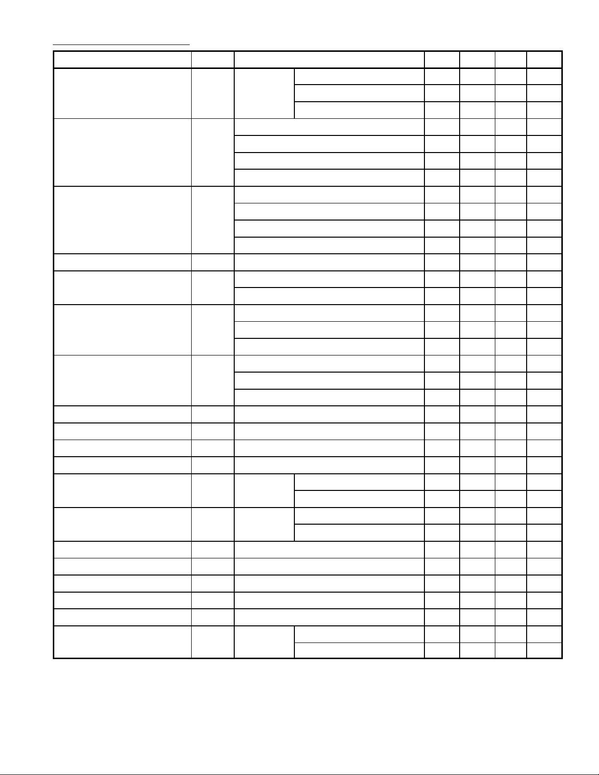
Electrical Characteristics: (V+ = ±15V, RL = 5kΩ to Pin7, TA = +25°C unless otherwise specified)
Parameter Symbol Test Conditions Min Typ Max Unit
Input Offset Voltage V
Input Offset Current I
Input Bias Current I
Input Resistance r
Large Signal Voltage Gain A
Positive Output Voltage Swing V
RS = 200Ω – 1.0 6.0 mV
IO
TA = 0° to +70°C – 1.0 9.0 mV
V+ = ±4V, RL = 10kΩ to Pin7 – – 6.0 mV
IO
– 50 750 nA
TA = +70°C – 0.5 1.5 µA
TA = 0°C – 0.5 1.5 µA
V+ = 4V, RL = 10kΩ to Pin7 – 50 600 µA
IB
– 0.3 1.5 µA
TA = +70°C – 0.3 3.0 µA
TA = 0°C – 0.3 3.0 µA
V+ = 4V, RL = 10kΩ to Pin7 – 0.3 1.5 µA
i
V
V
= ±10V 15000 50000 – V/V
OUT
V+ = ±4V, RL = 10kΩ to Pin7, V
O
= ±2V 15000 60000 – V/V
OUT
50 150 – kΩ
+12 +13 – V
TA = 0° to +70°C +12 +13 – V
V+ = ±4V, RL = 10kΩ to Pin7 +2.5 +2.8 – V
Negative Output Voltage Swing V
O
–14 –15 – V
TA = 0° to +70°C –14 –15 – V
V+ = ±4V, RL = 10kΩ to Pin7 –3.6 –4.0 – V
Output Resistance r
f = 1kHz – 5.0 – kΩ
o
Common Mode Rejection Ratio CMRR RS = 200Ω, VIN = +11.5V to –13.5V 70 90 – dB
Supply Voltage Rejection Ratio PSRR RS = 200Ω – 50 350 µV/V
Input Voltage Range V
I
Internal Power Dissipation V
= 0 – 180 330 mW
OUT
–13 – +11 V
V+ = ±4V, RL = 10kΩ to Pin7 – 20 – mW
Supply Current ICC, I
EEVOUT
= 0 – 9.0 14.0 mA
V+ = ±4V, RL = 10kΩ to Pin7 – 2.5 – mA
Broadband Noise Figure RS = 10kΩ, BW = 10H z to 10kHz – 2.5 – dB
Turn On Delay t
Turn Off Delay t
Open Loop, VIN = ±20mV – 0.2 – µs
on
Open Loop, VIN = ±20mV – 0.3 – µs
off
Slew Rate (Unity Gain) SR C1 = 0.02µF, R1 = 33Ω, C2 = 10pF – 1.0 – V/µs
Channel Separation RS = 1kΩ, f = 10kHz – 140 – dB
Input Offset Voltage Drift RS = 200Ω +25°C ≤ TA ≤ +70°C – 3.0 – µV/°C
0°C ≤ TA ≤ +25°C – 3.0 – µV/°C
 Loading...