

NTE NTE938, NTE938M Datasheet

NTE938 & NTE938M
Integrated Circuit
Precision Operational Amplifier
(OP Amp)
Description:
The NTE938 and NTE938M operational amplifiers provide high input impedance, low input offsets
and temperature drifts, and low noise. This series of amplifiers is particularly useful for applications
where high–accuracy and low–drift performance are essential. In addition, high–speed performance
may be improved by employing feed–forward compensation techniques to maximize slew rate without compromising other performance criteria.
The NTE938 and NTE938M offer extremely low input offset voltage and drift specifications allowing
usage in even the most critical applications without external offset nulling.
Features:
D Available in Two Packages Styles:
8–Lead Metal Can (NTE938)
8–Lead DIP (NTE938M)
D Operation From a Wide Range of Power Supply Voltages
D Low Input Bias and Offset Currents
D Low Input Offset Voltage and Guaranteed Offset Voltage Drift Performance
D High Input Impedance
Absolute Maximum Ratings:
Power Supply Voltage, V
Input Voltage (Note 1), V
Input Differential Current (Note 2), I
Output Short–Circuit Duration, t
Operating Junction Temperature, T
(TA = +25°C unless otherwise specified)
, V
CC
EE
I
ID
S
J
±18V. . . . . . . . . . . . . . . . . . . . . . . . . . . . . . . . . . . . . . . . . . . . . . . . . . . .
±15V. . . . . . . . . . . . . . . . . . . . . . . . . . . . . . . . . . . . . . . . . . . . . . . . . . . . . . . . . . .
±10mA. . . . . . . . . . . . . . . . . . . . . . . . . . . . . . . . . . . . . . . . . . . . . .
Indifinite. . . . . . . . . . . . . . . . . . . . . . . . . . . . . . . . . . . . . . . . . . . . . . . . .
NTE938 +175°C. . . . . . . . . . . . . . . . . . . . . . . . . . . . . . . . . . . . . . . . . . . . . . . . . . . . . . . . . . . . . . . . . .
NTE938M +150°C. . . . . . . . . . . . . . . . . . . . . . . . . . . . . . . . . . . . . . . . . . . . . . . . . . . . . . . . . . . . . . . .
Operating Ambient Temperature Range, T
Storage Temperature Range, T
stg
A
0° to +70°C. . . . . . . . . . . . . . . . . . . . . . . . . . . . . . . . . . . . .
–65° to +150°C. . . . . . . . . . . . . . . . . . . . . . . . . . . . . . . . . . . . . . . . . .
Note 1. For s upply v oltages l ess t han ±15V, the m aximum i nput v oltage i s e qual t o t he s upply v oltage.
Note 2. The inputs are shunted with back–to–back diodes for over–voltage protection. Therefore,
excessive current will flow if a differential input voltage in excess of 1.0V is applied between
the inputs unless some limiting resistance is used.
Electrical Characteristics: (TA = +25°C, 5V ≤ VCC ≤ 15V, –15V ≤ VEE ≤ –5V unless otherwise
specified)
Parameter Symbol Test Conditions Min Typ Max Unit
Input Offset Voltage V
IO
– 2.0 7.5 mV
TA = 0° to +70°C – – 10 mV
Input Offset Current I
IO
– 0.2 1.0 nA
TA = 0° to +70°C – – 1.5 nA
Input Bias Current I
IB
– 1.5 7.0 nA
TA = 0° to +70°C – – 10 nA
Input Resistance r
Power Supply Currents ICC, I
Large Signal Voltage Gain A
Average Temperature Coefficient of
VOL
∆VIO/∆T 0° ≤ TA ≤ +70°C – 6 30 µV/°C
I
EEVCC
= +15V, VEE = –15V – ±0.3 ±0.8 mA
VCC = +15V, VEE = –15V, VO = ±10V,
≥ 10kΩ
R
L
VCC = +15V, VEE = –15V, VO = ±10V,
R
≥ 10kΩ, TA = 0° to +70°C
L
10 40 – MΩ
25 300 – V/mV
15 – – V/mV
Input Offset Temperature
Average Temperature Coefficient of
∆IIO/∆T – 2 10 pA/°C
Input Offset Current
Input Voltage Range V
VCC = +15V, VEE = –15V ±14 – – V
IR
Common Mode Rejection Ratio CMRR RS ≤ 50kΩ 80 100 – dB
Supply Voltage Rejection Ratio PSRR RS ≤ 50kΩ 80 96 – dB
Output Voltage Range V
NTE938
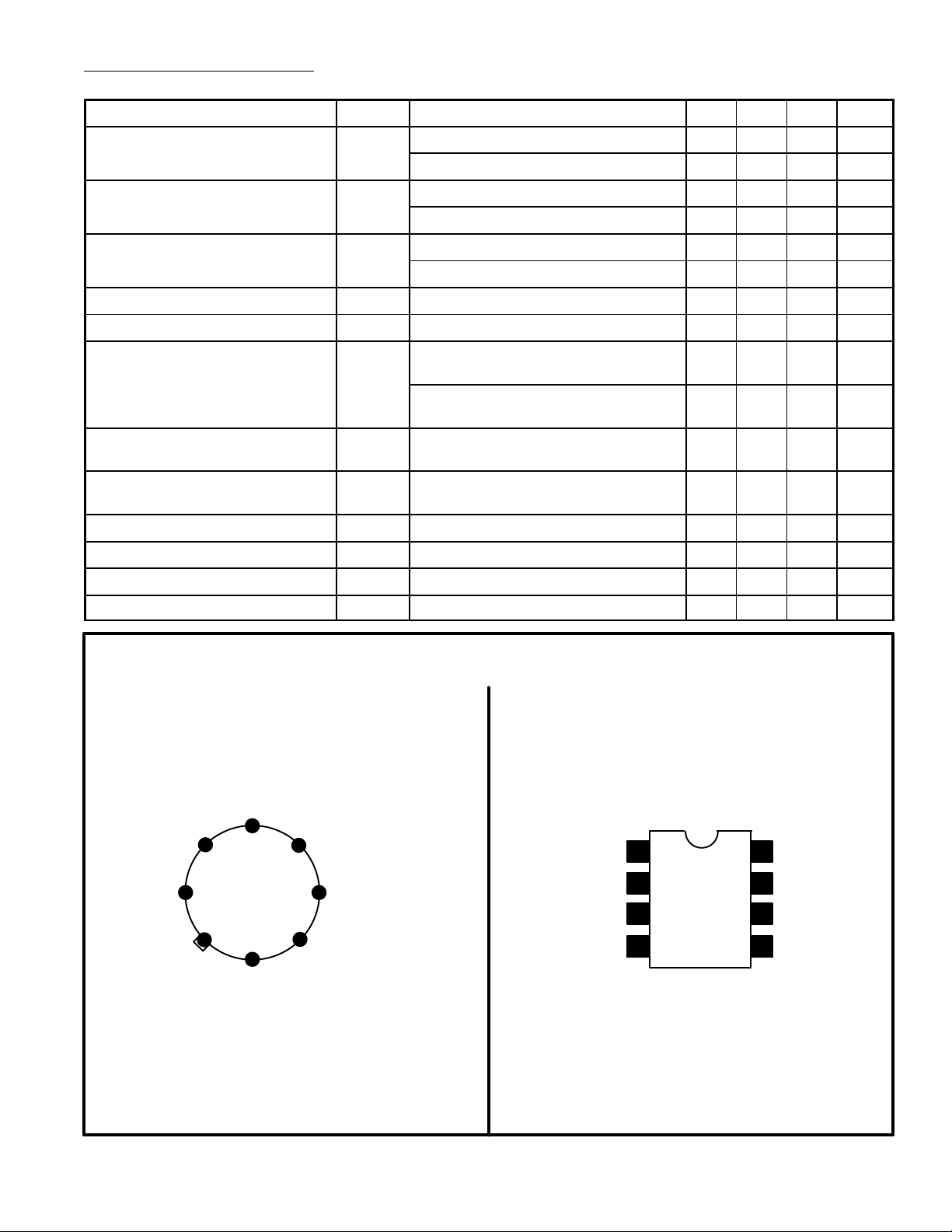
(Top View)
N.C.
Output
V (+)
7
Compensation 2
5
6
8
1
Compensation
1
V (–)
4
Non–Inverting Input
3
2
Inverting Input
OR
VCC = +15V, VEE = –15V, RL = 10kΩ ±13 ±14 – V
Pin Connection Diagram
Compensation 1
Invert Input12
Non–Inverting Input
V (–)
NTE938M
3
4
Compensation 2
8
V (+)
7
6
Output
5 N.C.
 Loading...