

NTE NTE937 Datasheet

NTE937
Integrated Circuit
JFET Input Operational Amplifier
Description:
The NTE937 is a monolithic JFET input operational amplifier in an 8–Lead Metal Can type package
incorporating well–matched, high voltage JFET’s on the same chip with standard bi–polar transistors.
This amplifier features low input bias and offset currents, low offset voltage and offset voltage drift,
coupled with offset adjust which does not degrade drift or common–mode rejection. It is also designed
for high slew rate, wide bandwidth, extremely fast settling time, low voltage and current noise and a
low 1/f noise corner.
Advantages:
D Replaces Expensive Hybrid and Module FET OP Amps
D Rugged JFET’s Allow Blow–Out Free Handling Compared with MOSFET Input Device
D Excellent for Low Noise Applications using either High or Low Source Impedance – Very Low
1/f Corner
D Offset Adjust does not Degrade Drift or Common–Mode Rejection as in Most Monolithic Amplifiers
D New Output Stage Allows use of Large Capacitive Loads (10,000pF) without Stability Problems
D Internal Compensation and Large Differential Input Voltage Capability
Applications:
D Precision High Speed Integrators
D Fast D/A and A/D Converters
D High Impedance Buffers
D Wideband, Low Noise, Low Drift Amplifiers
D Logarithmic Amplifiers
D Photocell Amplifiers
D Sample and Hold Circuits
Absolute Maximum Ratings:
Supply Voltage ±18V. . . . . . . . . . . . . . . . . . . . . . . . . . . . . . . . . . . . . . . . . . . . . . . . . . . . . . . . . . . . . . . . . . . .
Maximum Power Dissipation (at +25°C, Note 1), P
d
Differential Input Voltage ±30V. . . . . . . . . . . . . . . . . . . . . . . . . . . . . . . . . . . . . . . . . . . . . . . . . . . . . . . . . . .
Input Voltage Range (Note 2) ±16V. . . . . . . . . . . . . . . . . . . . . . . . . . . . . . . . . . . . . . . . . . . . . . . . . . . . . . .
Output Short–Circuit Duration Continuous. . . . . . . . . . . . . . . . . . . . . . . . . . . . . . . . . . . . . . . . . . . . . . . . .
Maximum Operating Junction Temperature (Note 1), T
Storage Temperature Range, T
Lead Temperature (During Soldering, 10sec), T
stg
L
Thermal Resistance, Junction–to–Ambient (Note 1), R
max +115°C. . . . . . . . . . . . . . . . . . . . . . . . . .
J
–65° to +150°C. . . . . . . . . . . . . . . . . . . . . . . . . . . . . . . . . . . . . . . . . .
thJC
Note 1. The maximum power dissipation for this device must be derated at elevated temperatures
and is dictated by T
max, R
J
power dissipation at any temperature is P
, and the ambient temperature, TA. The maximum available
thJC
= (TJmax – TA)/R
d
or the +25°C Pdmax, which-
thJC
ever is less.
Note 2. Unless otherwise specified, the absolute maximum negative input voltage is equal to the
negative power supply voltage.
570mW. . . . . . . . . . . . . . . . . . . . . . . . . . . . . . . . .
+300°C. . . . . . . . . . . . . . . . . . . . . . . . . . . . . . . . . . . .
+150°C/W. . . . . . . . . . . . . . . . . . . . . . . . .
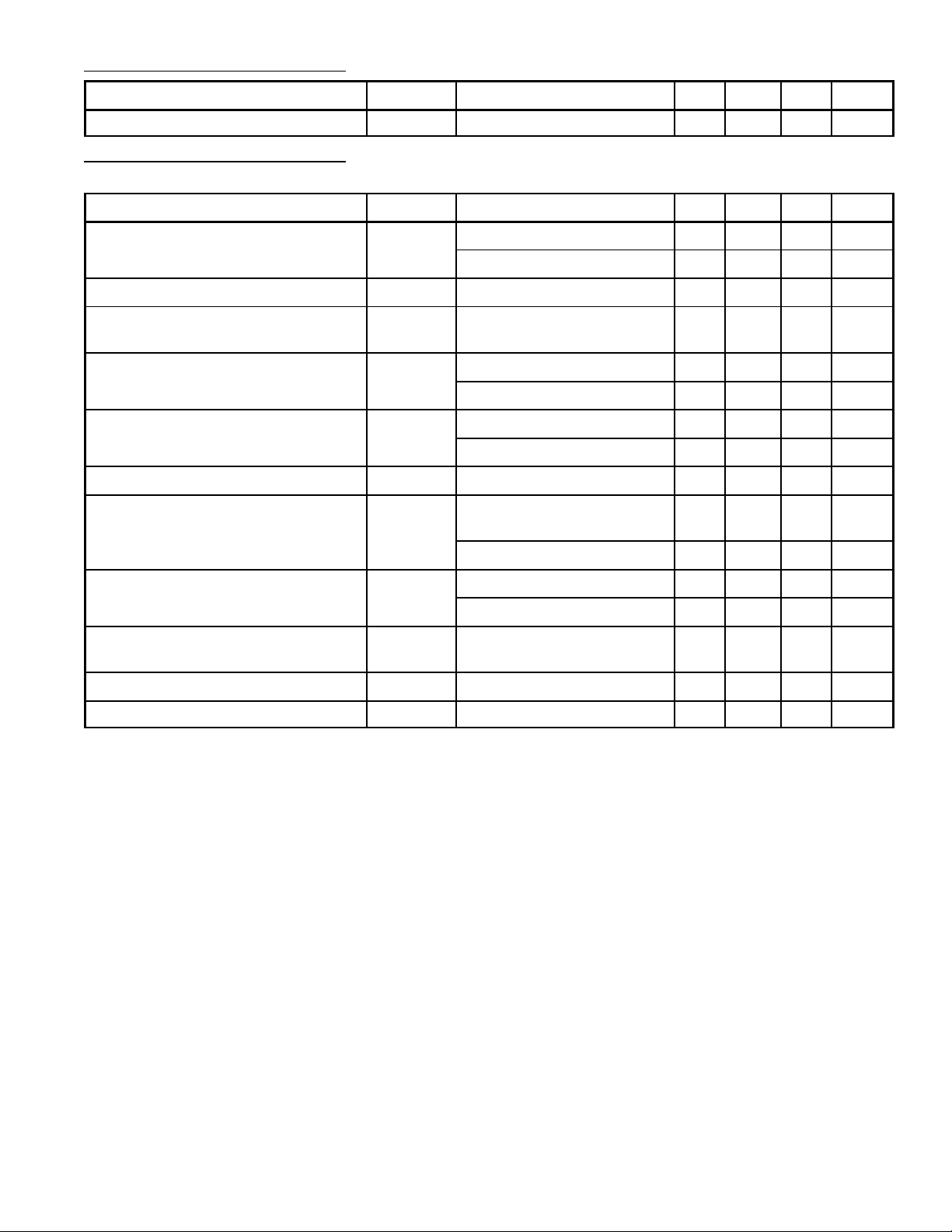
DC Electrical Characteristics: (TA = +25C, VS = ±15V unless otherwise specified)
Parameter Symbol Test Conditions Min Typ Max Unit
Supply Current I
CC
DC Electrical Characteristics: (VS = ±15V, 0° ≤ TA ≤ +70°C, T
HIGH
– 5 10 mA
= +70°C unles otherwise
specified)
Parameter Symbol Test Conditions Min Typ Max Unit
Input Offset Voltage V
OS
Average TC of Input Offset Voltage ∆VOS/∆T RS = 50Ω – 5 – µV/°C
Change in Average TC with V
OS
∆TC/∆V
Adjust
Input Offset Current I
Input Bias Current I
Input Resistance R
Large Signal Voltage Gain A
OS
B
IN
VOL
RS = 50Ω, TA = +25°C – 3 10 mV
Over Temperature – – 13 mV
OSRS
= 50Ω, Note 3 – 0.5 – µV/°C
TJ = +25°C, Note 4 – 3 50 pA
TJ ≤ T
HIGH
– – 2 nA
TJ = +25°C, Note 4 – 30 200 pA
TJ ≤ T
HIGH
TJ = +25°C – 10
TA = +25°C, VO = ±10V,
= 2k
R
L
– – 8 nA
12
– Ω
25 200 – V/mV
Over Temperature 15 – – V/mV
Output Voltage Swing V
O
RL = 10k ±12 ±13 – V
RL = 2k ±10 ±12 – V
Input Common–Mode Voltage Range V
CM
±10 +15.1
– V
–12
Common–Mode Rejection Ratio CMRR – 80 100 dB
Supply Voltage Rejection Ratio PSRR Note 5 – 80 100 dB
Note 3. The temperature coeficient of the adjust input offset voltage changes only a small amount
(0.5µV/°C typically) for each mV of adjustment from its original unadjusted value. Common–
mode rejection and open loop voltage gain are also unaffected by offset adjustment.
Note 4. The input bias currents are junction leakage currents which approximately double for every
10°C increase in the junction temperature, T
. Due to limited production test time, the input
J
bias currents measured are correlated to junction temperature. In normal operation the junction temperature rises above the ambient temperature as a result of internal power dissipation, P
. TJ = TA + R
d
thJC Pd
where R
is the thermal resistance from junction to ambient.
thJC
Use of a heat sink is recommended if input bias current is to be kept to a minimum.
Note 5. Supply Voltage Rejection is measured for both supply magnitudes increasing or decreasing
simultaneously, in accordance with common practice.
 Loading...