

NTE NTE935 Datasheet

NTE935
Integrated Circuit
3–Terminal Adjustable Positive Voltage Regulator
1.2V to 32V, 5A
Description:
The NTE935 is an adjustable 3–terminal positive voltage regulator in a TO3 type package capable
of supplying in excess of 5A over a 1.2V to 32V output range. This device is exceptionally easy to
use.
A unique feature of the NTE935 is its time dependent current limiting. The current limit circuitry allows
peak currents of up to 12A to be drawn from the regulator for short periods of time.
Also included on the chip are thermal overload protection and safe area protection for the p ower transistor.
Overload protection remains functional even if the adjustment pin is accidently disconnected.
Normally, no capacitors are needed unless the device is situated far from the input filter capacitors
in which case an input bypass is needed. An optional output capacitor can be added to improve transient response. The adjustment terminal can be bypassed to achieve very high ripple rejections ratios
which are difficult to achieve with standard 3–terminal regulators.
Features:
D Guaranteed 7A Peak Output Current
D Guaranteed 5A Output Current
D Adjustable Output Down to 1.2V
D Line Regulation Typically 0.005%/V
D Load Regulation Typically 0.1%
D Guaranteed Thermal Regulation
D Output is Short Circuit Protected
D Current Limit Constant with Temperature
D Standard 3–Lead Transistor Package.
Absolute Maximum Ratings:
Power Dissipation, P
Input–Output Voltage Differential, V
Operating Junction Temperature Range, T
Storage Temperature Range, T
D
I–O
J
stg
Lead Temperature (During Soldering, 10 seconds), T
Thermal Resistance, Junction–to–Case, R
Thermal Resistance, Junction–to–Ambient, R
thJC
thJA
Internally limited. . . . . . . . . . . . . . . . . . . . . . . . . . . . . . . . . . . . . . . . . . . . . . . . . . .
35V. . . . . . . . . . . . . . . . . . . . . . . . . . . . . . . . . . . . . . . . . . . . . . . .
0° to +125°C. . . . . . . . . . . . . . . . . . . . . . . . . . . . . . . . . . . .
–65° to +150°C. . . . . . . . . . . . . . . . . . . . . . . . . . . . . . . . . . . . . . . . . .
L
+300°C. . . . . . . . . . . . . . . . . . . . . . . . . . . . . . .
1.0°C/W. . . . . . . . . . . . . . . . . . . . . . . . . . . . . . . . . . . . .
35°C/W. . . . . . . . . . . . . . . . . . . . . . . . . . . . . . . . . . .
Electrical Characteristics: (+25°C ≤ TJ ≤ +150°C, VIN –V
= 5V and I
OUT
= 2.5A, Note 1
OUT
unless otherwise specified)
Parameter Test Conditions Min Typ Max Unit
Line Regulation 3V ≤ (VIN –V
3V ≤ (VIN –V
Load Regulation 10mA ≤ I
10mA ≤ I
OUT
OUT
Thermal Regulation Pulse = 20ms, TJ = +25°C – 0.002 0.02 %/W
Adjustment Pin Current – 45 100 µA
Adjustment Pin Current Change 10mA ≤ IL ≤ 5A, 3V ≤ (VIN – V
Reference Voltage 3 ≤ (VIN – V
Note 3
Temperature Stability T
Minimum Load Current (VIN –V
Current Limit (VIN – V
RMS Output Noise, % of V
OUTTJ
Ripple Rejection Ratio V
≤ TJ ≤ T
MIN
OUT
OUT
(VIN – V
OUT
= +25°C, 10Hz ≤ f ≤ 10kHz – 0.003 – %
= 10V, f = 120Hz – 60 – dB
OUT
C
= 10µF 60 75 – dB
ADJ
Long Term Stability TJ = +125°C – 0.3 1.0 %
≤ 35V, IL = 0.01A, Note 2 – 0.02 0.06 %/V
OUT)
≤ 35V, IL = 0.01A, TA = +25°C, Note 2 – 0.005 0.03 %/V
OUT)
≤ 5A, Note 2 – 0.3 1.0 %
≤ 5A, TA = +25°C, Note 2 – 0.1 0.5 %
) ≤ 35V – 0.2 5.0 µA
OUT
) ≤ 35V, 10mA ≤ I
OUT
MAX
≤ 5A, P ≤ 50W,
OUT
1.19 1.24 1.29 V
– 1 – %
) = 35V – 3.5 10 mA
) ≤10V 5.0 8.0 – A
) ≤ 30V – 1.0 – A
Note 1. Pow er di s s ipati o n is inte r n a l l y limi t ed, t h ese s p e cific ation s are appl i c a b le fo r powe r diss i p a tions
up to 50W.
Note 2. Regulation is measured at constant junction temperature. Changes in output voltage due
to heating effects are taken into account separately by thermal regulation.
Note 3. Selected devices with tightened tolerance reference voltage.
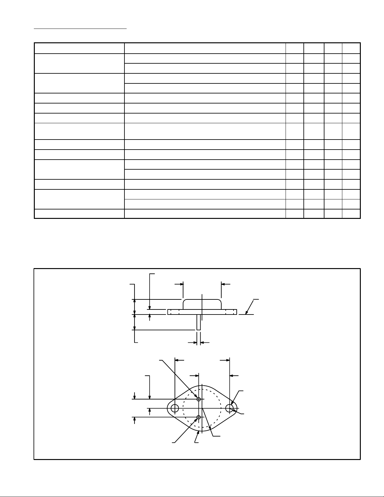
.135 (3.45) Max
.350 (8.89)
.215 (5.45)
.430
(10.92)
V
IN
.875 (22.2)
Dia Max
Seating Plane
.040 (1.02).312 (7.93) Min
1.187 (30.16)
.665
(16.9)
.156 (3.96) Dia
(2 Holes)
.188 (4.8) R Max
V
.525 (13.35) R Max
/CaseAdjust
OUT
 Loading...