

NTE NTE931 Datasheet

NTE931
Integrated Circuit
3–Terminal Positive Voltage Regulator
5V, 3A
Description:
The NTE931 is a 3–terminal fixed positive voltage regulator in a TO3 type package capable of driving
loads up to 3A. New circuit design and processing techniques are used to provide the high output
current without sacrificing the regulation characteristics of lower current devices.
This device is virtually blowout proof. Current limiting and thermal shutdown provide a high level of
reliability. No external components are required for operation of the NTE931, however, if the device
is more than 4 inches from the filter capacitor a 1µF solid tantalum capacitor should be used on the
input. A 0. 1 µF or larger capacitor may be used on the output to reduce load transient spikes created
by fast switching digital logic, or to swamp out stray load capacitance.
An overall worst case specification for the combined effects of input voltage, load current, ambient
temperature, and power dissipation ensures that the NTE931 will perform satisfactory as a system
element.
Features:
D Output Current in Excess of 3A
D Internal Current and Thermal Limiting
D 0.01Ω Typical Output Impedance
D 7.5 Minimum Input Voltage
D 30W Power Dissipation
D 100% Electrical Burn–In
Absolute Maximum Ratings:
Input Voltage, V
Power Dissipation, P
Operating Junction Temperature Range, T
Storage Temperature Range, T
Typical Thermal Resistance, Junction–to–Case (Note 1), R
Lead Temperature (Soldering, 10 sec), T
Burn–In In Thermal Limit 100%. . . . . . . . . . . . . . . . . . . . . . . . . . . . . . . . . . . . . . . . . . . . . . . . . . . . . . . . . .
Note 1. Without a h eatsink, thermal resistance is about 3 5°C/W . W ith a heatsink, the ef fective t hermal
resistance can o nly a pproach t he s pecified v alue o f 2°C/W, d epending o n t he e ffeciency o f t he
heatsink.
IN
D
J
stg
thJC
L
Internally Limited. . . . . . . . . . . . . . . . . . . . . . . . . . . . . . . . . . . . . . . . . . . . . . . . . .
0° to +125°C. . . . . . . . . . . . . . . . . . . . . . . . . . . . . . . . . . . .
–65° to +150°C. . . . . . . . . . . . . . . . . . . . . . . . . . . . . . . . . . . . . . . . . .
20V. . . . . . . . . . . . . . . . . . . . . . . . . . . . . . . . . . . . . . . . . . . . . . . . . . . . . . . . . . . . . . . . . .
2°C/W. . . . . . . . . . . . . . . . . . . . . . . . .
+300°C. . . . . . . . . . . . . . . . . . . . . . . . . . . . . . . . . . . . . . . . . .
Electrical Characteristics: (TJ = 0° to +125°C, Note 2 unless otherwise specified)
Parameter Symbol Test Conditions Min Typ Max Unit
Output Voltage V
TJ = +25°C, VIN = 7.5V, IO = 0A 4.8 5.0 5.2 V
O
VIN = 7.5V to 15V, IO = 0A to 3A, P ≤ 30W 4.75 5.00 5.25 V
Line Regulation Reg
Load Regulation Reg
Quiescent Current I
Output Noise Voltage V
lineTJ
loadTJ
B
n
= +25°C, VIN = 7.5V to 15V, Note 3 – 5 25 mV
= +25°C, VIN = 7.5V, IO = 0A to 3A, Note 3 – 25 100 mV
VIN = 7.5V to 15V, IO = 0A to 3A – 12 20 mA
TJ = +25°C, f = 10Hz to 100kHz – 40 – µV
rms
Short Circuit Current Limit TJ = +25°C, VIN = 15V – 3.0 4.5 A
TJ = +25°C, VIN = 7.5V – 4.0 5.0 A
Long Term Stability – – 35 mW
Note 2. Although power dissipation is internally limited, specifiecations apply only for P ≤ 30W.
Note 3. Load and line regulation are specified at constant junction temperature. Pulse testing is
required with a pulse width of ≤ 1ms and a duty cycle of ≤ 5%.
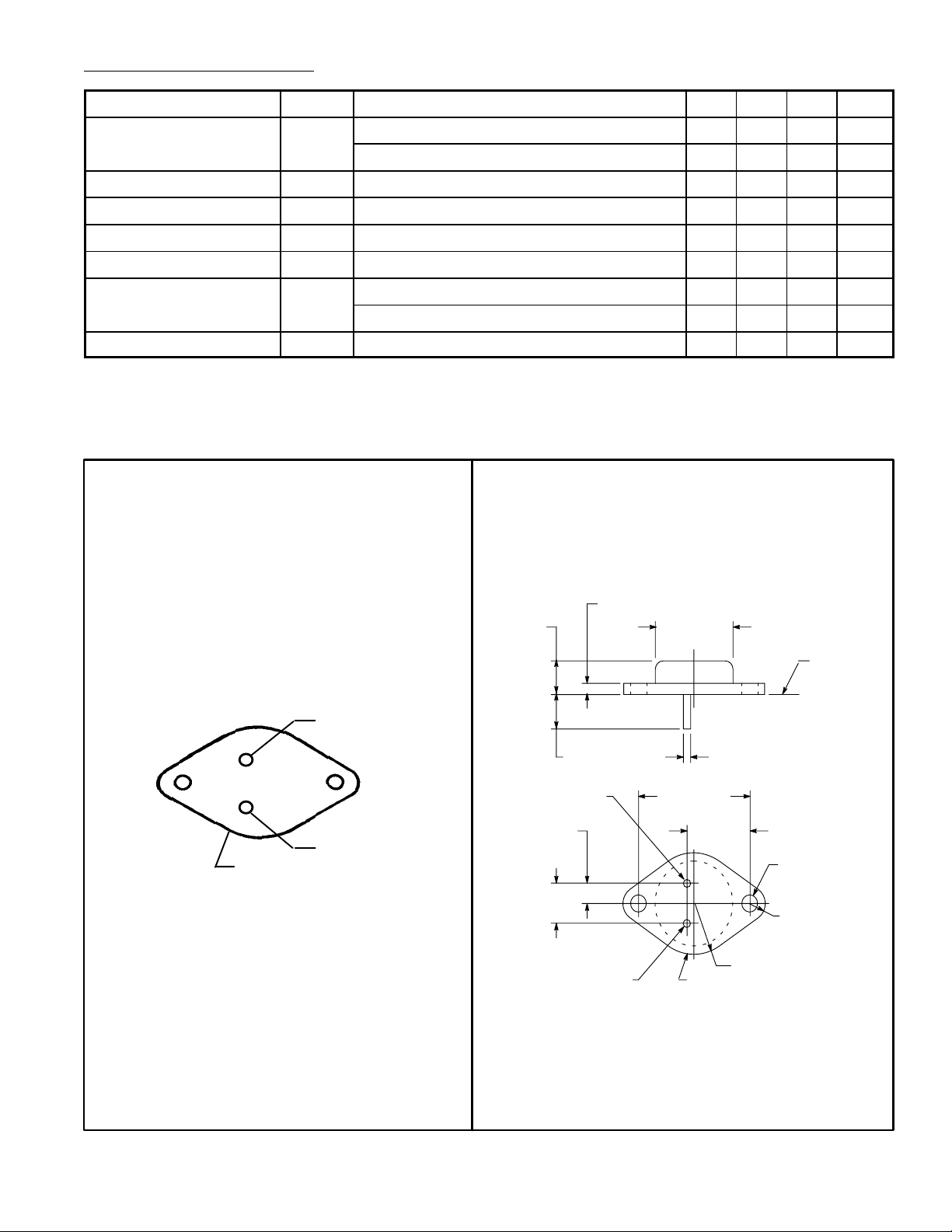
Pin Connection Diagram
2
1
Case/GND
Output
Input
.350 (8.89)
.215 (5.45)
.312 (7.93) Min
.430
(10.92)
.135 (3.45) Max
V
OUT
V
IN
.875 (22.2)
Dia Max
Seating
Plane
.040 (1.02)
1.187 (30.16)
.665
(16.9)
.156 (3.96) Dia
(2 Holes)
.188 (4.8) R Max
.525 (13.35) R Max
GND/Case
 Loading...