

NTE NTE929 Datasheet
NTE929
Integrated Circuit
General Purpose, High Current, NPN Transistor Array
Description:
The NTE929 is a versatile array of five high–current (to 100mA) NPN transistors on a common monolithic substrate. In addition, two of these transistors (Q1 and Q2) are matched at low currents (i.e.
1mA) for applications in which offset parameters are of special importance.
Independent connections for each transistors plus a separate terminal for the substrate permit maximum flexibility in circuit design.
Features
D High I
D Low V
:
100mA max
C
(at 50mA) 0.7V max.
CEsat
D Matched pair (Q1 and Q2)
V
(VBE matched): ±5mV max.
10
I
(at 1mA): 2.5µA max.
10
D 5 independent transistors plus separate substrate connection.
Applications:
D Signal processing and switching systems operating from DC to VHF
D Lamp and relay driver
D Differential amplifier
D Temperature–compensated amplifier
D Thyristor firing
Absolute Maximum Ratings
Power Dissipation, P
D
: (TA = +25°C unless otherwise specified)
Any One Transistor 500mW. . . . . . . . . . . . . . . . . . . . . . . . . . . . . . . . . . . . . . . . . . . . . . . . . . . . . . .
Total Package 750mW. . . . . . . . . . . . . . . . . . . . . . . . . . . . . . . . . . . . . . . . . . . . . . . . . . . . . . . . . . .
Derate Above 55°C Derate Linearly 6.67mW/°C. . . . . . . . . . . . . . . . . . . . . . . . . . . . . . . . . . .
Operating Ambient Temperature Range, T
Storage Temperature range, T
stg
opr
Lead Temperature (During Soldering, 1/16” ±1/32” from case, 10sec max), T
L
–55 to +125°C. . . . . . . . . . . . . . . . . . . . . . . . . . . . . . . . .
–65 to +150°C. . . . . . . . . . . . . . . . . . . . . . . . . . . . . . . . . . . . . . . . . . .
+265°C. . . . . . . . . . .
The following ratings apply for each transistor in the device:
Collector–Emitter Voltage, V
Collector–Base Voltage, V
CEO
CBO
Collector–Substrate Voltage, V
Emitter–Base Voltage, V
Collector Current, I
Base Current, I
B
EBO
C
CIO
15V. . . . . . . . . . . . . . . . . . . . . . . . . . . . . . . . . . . . . . . . . . . . . . . . . . . . . .
20V. . . . . . . . . . . . . . . . . . . . . . . . . . . . . . . . . . . . . . . . . . . . . . . . . . . . . . .
20V. . . . . . . . . . . . . . . . . . . . . . . . . . . . . . . . . . . . . . . . . . . . . . . . . . . .
5V. . . . . . . . . . . . . . . . . . . . . . . . . . . . . . . . . . . . . . . . . . . . . . . . . . . . . . . . . .
20mA. . . . . . . . . . . . . . . . . . . . . . . . . . . . . . . . . . . . . . . . . . . . . . . . . . . . . . . . . . . . . .
20mA. . . . . . . . . . . . . . . . . . . . . . . . . . . . . . . . . . . . . . . . . . . . . . . . . . . . . . . . . . . . . . . . .
Note 1. The collector of each transistor of the NTE929 is isolated from the substrate by an integral
diode. The substrate must be connected to a voltage which is more negative than any collector voltage in order to maintain isolation between transistors and provide normal transistor
action. To avoid undesired coupling between transistors, the substrate terminal (Pin5)
should be maintained at either DC or signal (AC) ground. A suitable bypass capacitor can
be used to establish a signal ground.
Electrical Characteristics: (TA = +25°C unless otherwise specified)
Parameter Symbol Test Conditions Min Typ Max Unit
For Each Transistor
Collector–Base Breakdown Voltage V
Collector–Emitter Breakdown Voltage V
Collector–Substrate Breakdown Voltage V
Emitter–Base Breakdown Voltage V
(BR)CBOIC
(BR)CEOIC
(BR)CIOICI
(BR)EBOIE
Collector Cutoff Current I
I
DC Forward Current h
Base–Emitter Voltage V
Collector–Emitter Saturation Voltage V
CE(sat)IC
Gain–Bandwidth Product f
Absolute Input Offset Voltage V
Absolute Input Offset Current I
Collector Q
Collector Q
Base Q
Emitter Q
Base Q
Collector Q
Emitter Q
= 100µA, IE = 0 20 60 – V
= 1mA, IB = 0 15 24 – V
= 100µA, IB = 0, IE = 0 20 60 – V
= 500µA, IC = 0 5.0 6.9 – V
CEO
CBO
FE
VCE = 10V, IB = 0 – – 10 µA
VCE = 10V, IE = 0 – – 1 µA
VCE = 3V, IC = 10mA 40 76 –
VCE = 3V, IC = 50mA 40 75 –
BE
VCE = 3V, IC = 10mA 0.65 0.74 0.85 V
= 50mA, IB = 5mA – 0.4 0.7 V
T
IO
IO
VCE = 3V, IC = 10mA – 450 – MHz
VCE = 3V, IC = 1mA – 1.2 5.0 mV
VCE = 3V, IC = 1mA – 0.7 2.5 µA
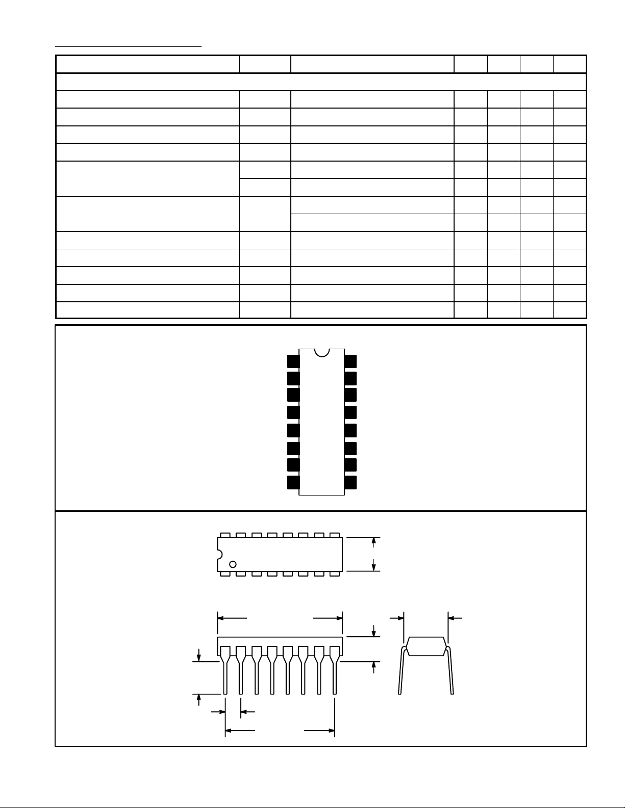
Pin Connection Diagram
1
1
2
2
3
2
4
2
5Substrate
6
3
7
3
8
3
Base Q
16
Emitter Q
15
Collector Q
14
Base Q
13
Emitter Q
12
Emitter Q
11
Base Q
10
Collector Q
9
1
1
5
5
5
4
4
4
.245
(6.22)
Min
16 9
.260 (6.6) Max
18
.785 (19.9)
Max
.200 (5.08)
Max
.100 (2.54)
.700 (17.7)
.300
(7.62)
 Loading...