

NTE NTE928S Datasheet
NTE928S
Integrated Circuit
Low Power Dual Operational Amplifier
Description:
Utilizing the circuit designs perfected for recently introduced Quad Operational Amplifiers, the
NTE928S dual operational amplifier features low power drain, a common mode input voltage range
extending to ground/V
This amplifier has several distinct advantages over standard operational amplifier types in single supply applications. It can operate at supply voltages as low as 3.0 V olts or as high as 32 Volts with quiescent currents about one–fifth of those associated with the NTE941 (on a per amplifier basis). The
common mode input range includes the negative supply , thereby eliminating the necessity for external biasing power supply voltage.
Features:
D Short Circuit Protected Outputs
D True Differential Input Stage
D Single Supply Operation: 3.0 to 32 Volts
D Low Input Bias Currents
D Internally compensated
D Common Mode Range Extends to Negative Supply
D Single and Split Supply Operation
, and Single Supply or Split Supply Operation.
EE
Maximum Ratings:
Power Supply Voltages
Single Supply, V
Split Supplies, V
Input Differential Voltage Range (Note 1), V
CC
CC VEE
IDR
Input Common Mode Voltage Range (Note 2), V
Input Forward Current (V
Output Short Circuit Duration, t
Junction Temperature, T
Operating Ambient Temperature Range, T
–0.3V, Note 3), I
I
S
J
IF
A
ICR
–0.3 to 32V. . . . . . . . . . . . . . . . . . . . . . . . . . . . . .
Continuous. . . . . . . . . . . . . . . . . . . . . . . . . . . . . . . . . . . . . . . . . . . . . . .
–55° to +125°C. . . . . . . . . . . . . . . . . . . . . . . . . . . . . . . . . . . . . . . . . . . . . . . . . .
0° to +70°C. . . . . . . . . . . . . . . . . . . . . . . . . . . . . . . . . . . . .
32V. . . . . . . . . . . . . . . . . . . . . . . . . . . . . . . . . . . . . . . . . . . . . . . . . . . . . . . . . . .
±16V. . . . . . . . . . . . . . . . . . . . . . . . . . . . . . . . . . . . . . . . . . . . . . . . . . . . . .
±32V. . . . . . . . . . . . . . . . . . . . . . . . . . . . . . . . . . . . . . . .
50mA. . . . . . . . . . . . . . . . . . . . . . . . . . . . . . . . . . . . . . . . .
Note 1. Split Power Supplies
Note 2. For supply voltages less than 32V, the absolute maximum input voltage is equal to the supply
voltage.
Note 3. This input current will only exist when the voltage is negative at any of the input leads. Normal
output states will reestablish when the input voltage returns to a voltage greater than 0.3V.
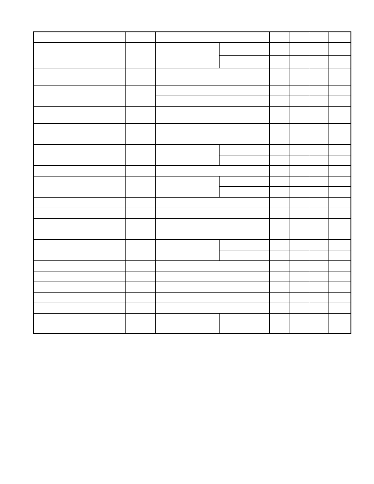
Electrical Characteristics: (VCC = 5V, VEE = Gnd, TA = +25°C unless otherwise specified)
Parameter Symbol Test Conditions Min Typ Max Unit
Input Offset Voltage V
Average Temperature Coefficient
∆VIO/∆T 0° ≤ TA ≤ +70°C – 7.0 – µV/°C
VCC = 5V to 30V,
IO
VIC =0 to VCC–1.7V,
VO ] 1.4V, RS = 0Ω
0° ≤ TA ≤ +70°C – – 9.0 mV
– 2.0 7.0 mV
of Input Offset Voltage
Input Offset Current I
IO
– 5.0 50 nA
0° ≤ TA ≤ +70°C – – 150 nA
Average Temperature Coefficient
∆IIO/∆T 0° ≤ TA ≤ +70°C – 10 – pA/°C
of Input Offset Current
Input Bias Current I
IB
– –45 –250 nA
0° ≤ TA ≤ +70°C – –50 –500 nA
Input Common–Mode Voltage V
ICR
VCC = 30V, Note 4
Range
Differential Input Voltage Range V
Large Signal Open–Loop A
IDR
VOL
RL = 2kΩ, VCC = 15V,
Voltage Gain For Large VO Swing
0° ≤ TA ≤ +70°C 0 – 28 V
0° ≤ TA ≤ +70°C 15 – – V/mV
0 – 28.3 V
– – V
CC
V
25 100 – V/mV
Channel Separation 1kHz ≤ f ≤ 20kHz, Input Referenced – –120 – dB
Common–Mode Rejection Ratio CMRR RS ≤ 10kΩ 65 70 – dB
Power Supply Rejection Ratio PSRR 65 100 – dB
Output Voltage Range V
Output Voltage – High Limit V
Output Voltage – Low Limit V
Output Source Current I
Output Sink Current I
OR
OH
OL
O+
O–
RL = 2kΩ 0 – 3.3 V
VCC = 30V,
0° ≤ TA ≤ +70°C
RL = 2kΩ 26 – – V
RL = 10kΩ 27 28 – V
VCC = 5V, RL = 10kΩ, 0° ≤ TA ≤ +70°C – 5 20 mV
VID = +1V, VCC = 15V 20 40 – mA
VID = –1V, VCC = 15V 10 20 – mA
VID = –1V, VO = 200mV 12 50 – µA
Output Short–Circuit to GND I
Power Supply Current I
os
CC
Note 5 – 40 60 mA
VO = 0, RL = ∞,
0° ≤ TA ≤ +70°C
VCC = 30V – 1.5 3.0 mA
VCC = 5V – 0.7 1.2 mA
Note 4. The input common–mode voltage or either input signal voltage should not be allowed to go
negative by more than 0.3V. The upper end of the common–mode voltage range is
V
–1.7V, but either or both inputs can goto +32V without damage.
CC
Note 5. Short circuit from the output to V
can cause excessive heating and eventual destruction.
CC
Destructive dissipation can result from simultaneous shorts on all amplifiers.
 Loading...