

NTE NTE927D, NTE927SM Datasheet

NTE927D & NTE927SM
Integrated Circuit
Differential Video Amplifier
Description:
The NTE927D and NTE927SM are two–stage, differential input, differential output, wide–band video
amplifiers. The use of internal series–shunt feedback gives wide band bandwidth with low phase distortion and high gain stability. Emitter–follower outputs provide a high current drive, low impedance
capability . Its 120MHz bandwidth and selectable gains of 10, 100, and 400, without need for frequency compensation, make it a very useful circuit for memory element drivers, pulse amplifiers, and wide
band gain stages.
Features:
D 120MHz Bandwidth
D 250kΩ Input Resistance
D No Frequency Compensation Required
D Selectable Gains of 10, 100 and 400
D High Common Mode Rejection Ratio at High Frequencies
Applications:
D Magnetic Tape Systems
D Disk File Memories
D Thin and Thick Film Memories
D Woven and Plated Wire Memories
D Wide Band Video Amplifiers
Absolute Maximum Ratings:
Differential Input Voltage ±5V. . . . . . . . . . . . . . . . . . . . . . . . . . . . . . . . . . . . . . . . . . . . . . . . . . . . . . . . . . . .
Common Mode Input Voltage ±6V. . . . . . . . . . . . . . . . . . . . . . . . . . . . . . . . . . . . . . . . . . . . . . . . . . . . . . . .
Supply Voltage, V
Output Current, I
Power Dissipation (Note 1), P
Junction Temperature, T
Storage Temperature Range, T
Operating Temperature Range, T
CC
O
D
J
stg
opr
Lead Temperature (Soldering, 10sec), T
–65° to +150°C. . . . . . . . . . . . . . . . . . . . . . . . . . . . . . . . . . . . . . . . . .
0° to +70°C. . . . . . . . . . . . . . . . . . . . . . . . . . . . . . . . . . . . . . . . . . .
L
±8V. . . . . . . . . . . . . . . . . . . . . . . . . . . . . . . . . . . . . . . . . . . . . . . . . . . . . . . . . . . . . . . .
10mA. . . . . . . . . . . . . . . . . . . . . . . . . . . . . . . . . . . . . . . . . . . . . . . . . . . . . . . . . . . . . . . .
500mW. . . . . . . . . . . . . . . . . . . . . . . . . . . . . . . . . . . . . . . . . . . . . . . . . . .
+100°C. . . . . . . . . . . . . . . . . . . . . . . . . . . . . . . . . . . . . . . . . . . . . . . . . . . . . . . . .
+260°C. . . . . . . . . . . . . . . . . . . . . . . . . . . . . . . . . . . . . . . . . . .
Note 1. For operation at elevated temperatures, derate device based on a thermal resistance of
+150°C/W junction to ambient or +45°C/W junction to case.
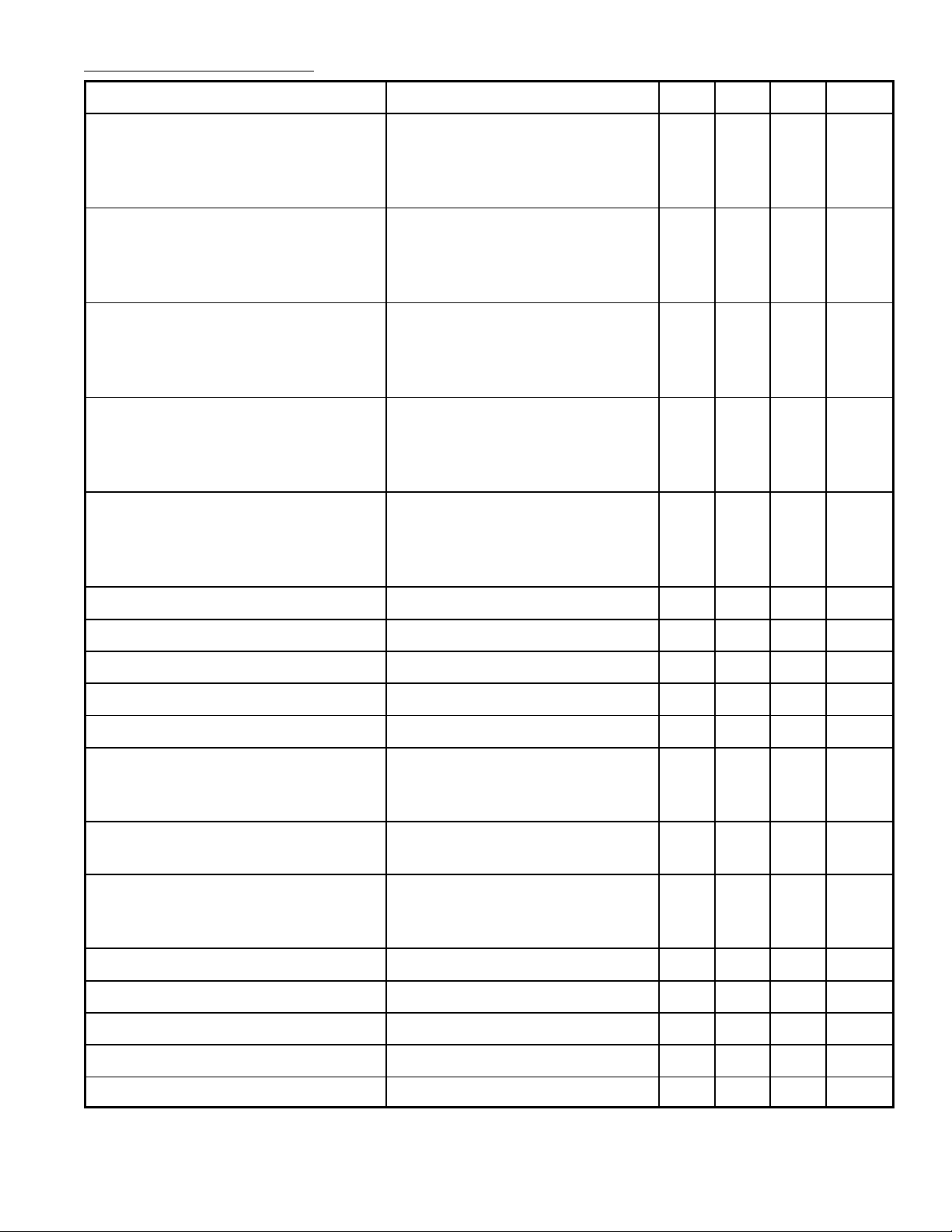
Electrical Characteristics: (TA = +25°C, unless otherwise specified, VS = ±6V)
Parameter
Differential Voltage Gain
Gain 1 (Note 2)
Gain 2 (Note 3)
Gain 3 (Note 4)
Bandwidth
Gain 1
Gain 2
Gain 3
Rise Time
Gain 1
Gain 2
Gain 3
Propagation Delay
Gain 1
Gain 2
Gain 3
Input Resistance
Gain 1
Gain 2
Gain 3
Test Conditions Min Typ Max Unit
RL = 2kΩ, V
V
= 1V
OUT
OUT
p–p
= 3V
p–p
250
80
8.0
–
–
–
–
–
–
–
–
–
–
10
–
400
100
10
40
90
120
10.5
4.5
2.5
7.5
6.0
3.6
4.0
30
250
600
120
12
MHz
–
–
–
ns
–
–
–
ns
–
10
–
kΩ
–
–
–
Input Capacitance Gain 2 – 2.0 – pF
Input Offset Current – 0.4 5.0 µA
Input Bias Current – 9.0 30 µA
Input Noise Voltage BW = 1kHz to 10MHz – 12 – µVrms
Input Voltage Range ±1.0 – – V
Common Mode Rejection Ratio
Gain 2
Gain 2
Supply Voltage Rejection Ratio
Gain 2
Output Offset Voltage
Gain 1
Gain 2 and 3
VCM = ±1V, f ≤ 100kHz
V
= ±1V, f = 5MHz
CM
60
–
86
60
∆VS = ±0.5V 50 70 –
RL = ∞ –
–
0.6
0.35
1.5
1.5
–
–
dB
dB
V
Output Common Mode Voltage RL = ∞ 2.4 2.9 3.4 V
Output Voltage Swing RL = 2k 3.0 4.0 –
Output Sink Current 2.5 3.6 – mA
Output Resistance – 20 – Ω
Power Supply Current RL = ∞ – 18 24 mA
 Loading...