

NTE NTE924, NTE924M Datasheet

NTE924 & NTE924M
Integrated Circuit
Voltage Follower, Operational Amplifier
Description:
The NTE924 and NTE924M are monolithic operational amplifiers internally connected as unity–gain
non–inverting amplifiers. These devices use super–gain transistors in the input stage to get low bias
current without sacrificing speed. Directly interchangeable with the NTE909 and NTE941 series in
voltage follower applications, these devices have internal frequency compensation and provision for
offset balancing.
Features:
D Available in 8–Lead DIP (NTE924M) and 8–Lead Metal Can (NTE924) Packages
D Input Current: 10nA Max Over Temperature
D Small Signal Bandwidth: 20MHz
D Slew Rate: 30V/µs
D Supply Voltage Range: ±5V to ±18V
Absolute Maximum Ratings:
Supply Voltage ±18V. . . . . . . . . . . . . . . . . . . . . . . . . . . . . . . . . . . . . . . . . . . . . . . . . . . . . . . . . . . . . . . . . . . .
Power Dissipation (Note 2), P
Input Voltage (Note 3) ±15V. . . . . . . . . . . . . . . . . . . . . . . . . . . . . . . . . . . . . . . . . . . . . . . . . . . . . . . . . . . . .
Output Short–Circuit Duration (Note 4) Indefinite. . . . . . . . . . . . . . . . . . . . . . . . . . . . . . . . . . . . . . . . . . .
Operating Temperature Range, T
Storage Temperature Range, T
Lead Temperature (During Soldering, 10sec), T
D
opr
stg
L
–65° to +150°C. . . . . . . . . . . . . . . . . . . . . . . . . . . . . . . . . . . . . . . . . .
500mW. . . . . . . . . . . . . . . . . . . . . . . . . . . . . . . . . . . . . . . . . . . . . . . . . . . .
0° to +70°C. . . . . . . . . . . . . . . . . . . . . . . . . . . . . . . . . . . . . . . . . . .
+260°C. . . . . . . . . . . . . . . . . . . . . . . . . . . . . . . . . . . .
Note 1. The NTE924M is a discontinued device and no longer available.
Note 2. For operating at elevated temperatures, the NTE924 must be derated based on a thermal
resistance of +150°C/W, junction–to–ambient, or +45°C/W, junction–to–case. The thermal
resistance of the NTE924M is +100°C/W, junction–to–ambient.
Note 3. For suppl y v oltages l ess than ±15V, t he a bsolute m axim um input v oltage i s e qual t o t he supply
voltage.
Note 4. Continuous short–circuit is allowed for case temperatures to +70°C or +55°C ambient tem-
perature. It is necessary to insert a resistor greater than 2kΩ in series with the input when
the amplifier is driven from low impedance sources to prevent damage when the output is
shorted. RS = 5k min, 14k typical is recommended for dynamic stability in all applications.
Electrical Characteristics: (±5V ≤ VS ≤ ±18V, 0° ≤ TA ≤ +70°C unless otherwise specified)
Parameter Test Conditions Min Typ Max Unit
Input Offset Voltage TA = +25°C – 2.5 7.5 mV
– – 10 mV
Input Bias Current TA = +25°C – 2.0 7.0 nA
– – 10 nA
Input Resistance TA = +25°C 10
Input Capacitance – 1.5 – pF
10
10
12
–
Ω
Large Signal Voltage Gain TA = +25°C, VS = ±15V, V
VS = ±15V, V
Output Resistance TA = +25°C – 0.75 2.5
Supply Current TA = +25°C – 3.9 5.5 mV
Temperature Drift – 10 – µV/°C
Output Voltage Swing VS = ±15V, RL = 10kΩ, Note 5 ±10 – – V
Supply Voltage Rejection Ratio ±5V ≤ VS ≤ ±18V 70 80 – dB
= ±10V, RL = 10kΩ 0.999 – – V/V
OUT
= ±10V, RL = 8kΩ 0.999 0.9999 – V/V
OUT
Ω
Note 5. Increased output swing under load can be obtained by connecting an external resistor
between the booster and V (–) terminals.
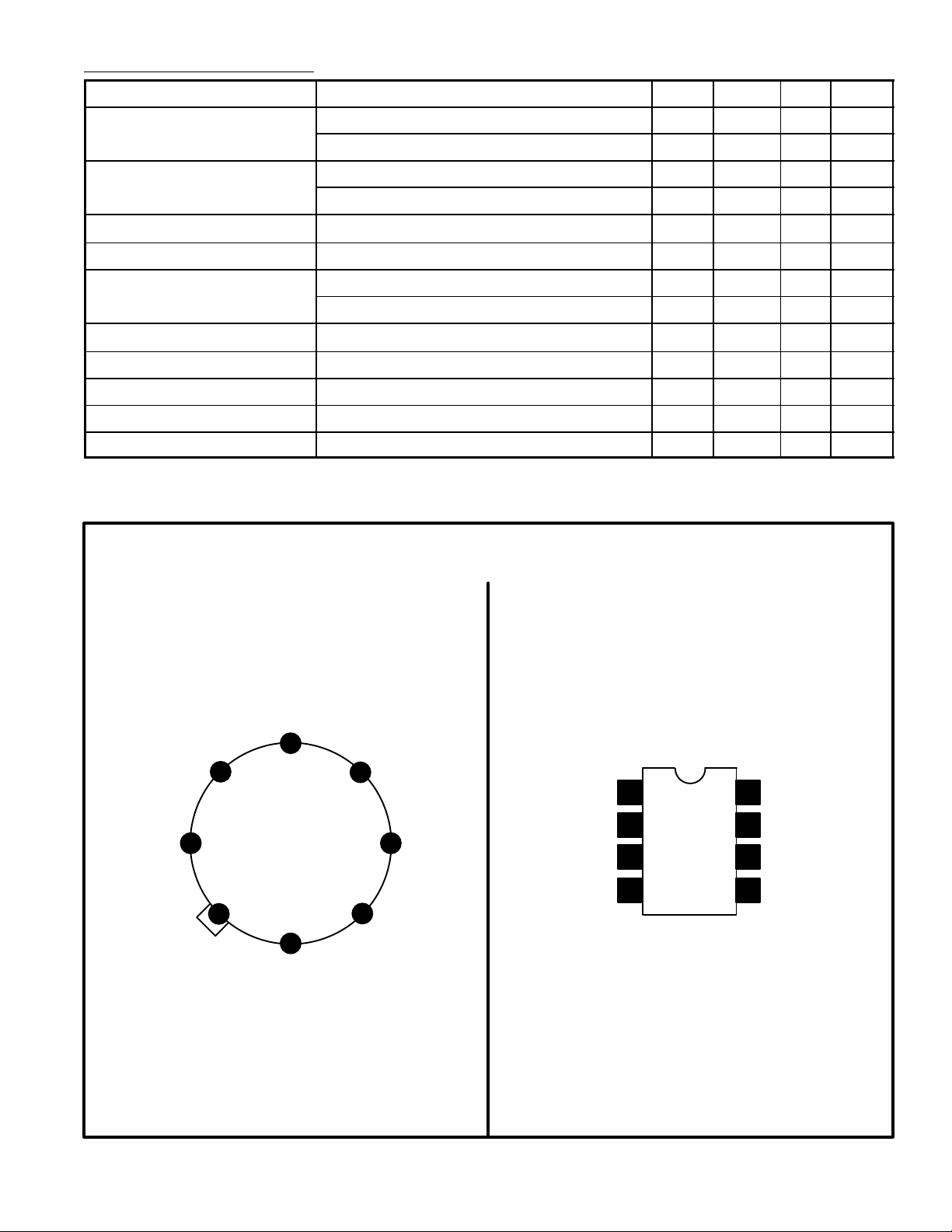
Pin Connection Diagram
NTE924
(Top View)
Booster
NTE924M
V (+)
Balance
Output
7
5
6
8
1
Balance
V (–)
4
Balance
Input
3
2
N.C.
N.C.
Input
V (–)
2
3
4
8
7
6
5
Balance1
V (+)
Output
Booster
 Loading...