

NTE NTE923D, NTE923 Datasheet

NTE923 & NTE923D
Integrated Circuit
Precision Voltage Regulator
Description:
The NTE923 and NTE923D are voltage regulators designed primarily for series regulator applications. By themselves, these devices will supply output currents up to 150mA; but, external transistors
can be added to provide any desired load current. The circuits feature extremely low standby current
drain, and provision is made for either linear or foldback current limiting.
These devices are also useful in a wide range of other applications such as shunt regulators, current
regulators, and temperature controllers.
Features:
D 150mA Output Current without External Pass Transistor
D Output Currents in Excess of 10A Possible by Adding External Transistors
D Input Voltage: 40V Max
D Output Voltage Adjustable from 2V to 37V
D Can be Used as Either a Linear or a Switching Regulator
Absolute Maximum Ratings:
Pulse Voltage from V+ to V– (50ms) 50V. . . . . . . . . . . . . . . . . . . . . . . . . . . . . . . . . . . . . . . . . . . . . . . . . .
Continuous Voltage from V+ to V– 40V. . . . . . . . . . . . . . . . . . . . . . . . . . . . . . . . . . . . . . . . . . . . . . . . . . . .
Input–Output Voltage Differential 40V. . . . . . . . . . . . . . . . . . . . . . . . . . . . . . . . . . . . . . . . . . . . . . . . . . . . .
Maximum Amplifier Input Voltage
Either Input 8.5V. . . . . . . . . . . . . . . . . . . . . . . . . . . . . . . . . . . . . . . . . . . . . . . . . . . . . . . . . . . . . . . . .
Differential 5.0V. . . . . . . . . . . . . . . . . . . . . . . . . . . . . . . . . . . . . . . . . . . . . . . . . . . . . . . . . . . . . . . . .
Current from V
Current from V
Internal Power Dissipation
NTE923 800mW. . . . . . . . . . . . . . . . . . . . . . . . . . . . . . . . . . . . . . . . . . . . . . . . . . . . . . . . . . . . . . . . .
NTE923D 660mW. . . . . . . . . . . . . . . . . . . . . . . . . . . . . . . . . . . . . . . . . . . . . . . . . . . . . . . . . . . . . . .
Operating Temperature Range 0° to +70°C. . . . . . . . . . . . . . . . . . . . . . . . . . . . . . . . . . . . . . . . . . . . . . . .
Storage Temperature Range
NTE923 –65° to +150°C. . . . . . . . . . . . . . . . . . . . . . . . . . . . . . . . . . . . . . . . . . . . . . . . . . . . . . . . . . .
NTE923D –55° to +150°C. . . . . . . . . . . . . . . . . . . . . . . . . . . . . . . . . . . . . . . . . . . . . . . . . . . . . . . . .
Lead Temperature (During Soldering, 4sec max)
NTE923 +300°C. . . . . . . . . . . . . . . . . . . . . . . . . . . . . . . . . . . . . . . . . . . . . . . . . . . . . . . . . . . . . . . . . .
NTE923D +260°C. . . . . . . . . . . . . . . . . . . . . . . . . . . . . . . . . . . . . . . . . . . . . . . . . . . . . . . . . . . . . . . .
Z
REF
25mA. . . . . . . . . . . . . . . . . . . . . . . . . . . . . . . . . . . . . . . . . . . . . . . . . . . . . . . . . . . . . . . . . .
15mA. . . . . . . . . . . . . . . . . . . . . . . . . . . . . . . . . . . . . . . . . . . . . . . . . . . . . . . . . . . . . . . .
Electrical Characteristics: (Note 1)
Parameter Test Conditions Min Typ Max Unit
Line Regulation VIN = 12V to 15V – 0.01 0.1 % V
0° ≤ TA ≤ +70°C – – 0.3 % V
VIN = 12V to 40V – 0.1 0.5 % V
Load Regulation IL = 1mA to 50mA – 0.03 0.2 % V
0° ≤ TA ≤ +70°C – – 0.6 % V
Ripple Rejection f = 50Hz to 10kHz C
Average Temperature Coefficient of
0° ≤ TA ≤ +70°C, Note 2 – 0.003 0.015 %/°C
= 0 – 74 – dB
REF
C
= 5µF – 86 – dB
REF
OUT
OUT
OUT
OUT
OUT
Output Voltage
Short Circuit Current Limit RSC = 10Ω, V
= 0 – 65 – mA
OUT
Reference Voltage 6.80 7.15 7.50 V
Output Noise Voltage BW = 100Hz to 10kHz C
= 0 – 86 – µV
REF
C
= 5µF – 2.5 – µV
REF
rms
rms
Long Term Stability – 0.05 – %/1000Hrs
Standby Current Drain IL = 0, VIN = 30V – 1.7 4.0 mA
Input Voltage Range 9.5 – 40 V
Output Voltage Range 2.0 – 37 V
Input–Output Voltage Differential 3.0 – 38 V
Thermal Resistance, Junction to Ambient
NTE923D
– 105 – °C/W
NTE923 Board mount in still air – 225 – °C/W
Board mount in 400LF/Min Air flow – 90 – °C/W
Thermal Resistance, Junction to Case – 25 – °C/W
Note 1. Unless otherwise otherwise specified, TA = +25°C, VIN = V+ = VC = 12V, V– = 0, V
I
= 1mA, RSC = 0, C! = 100pF, C
L
= 0 and divider impedance as seen by error amplifier
REF
OUT
≤ 10kΩ. Line and load regulation specifications are given for the condition of constant chip
temperature. Temperature drifts must be taken into account separately for high dissipation
conditions.
Note 2. Guaranteed by correlation to other tests.
Note 3. For metal can applications where V
nected in series with V
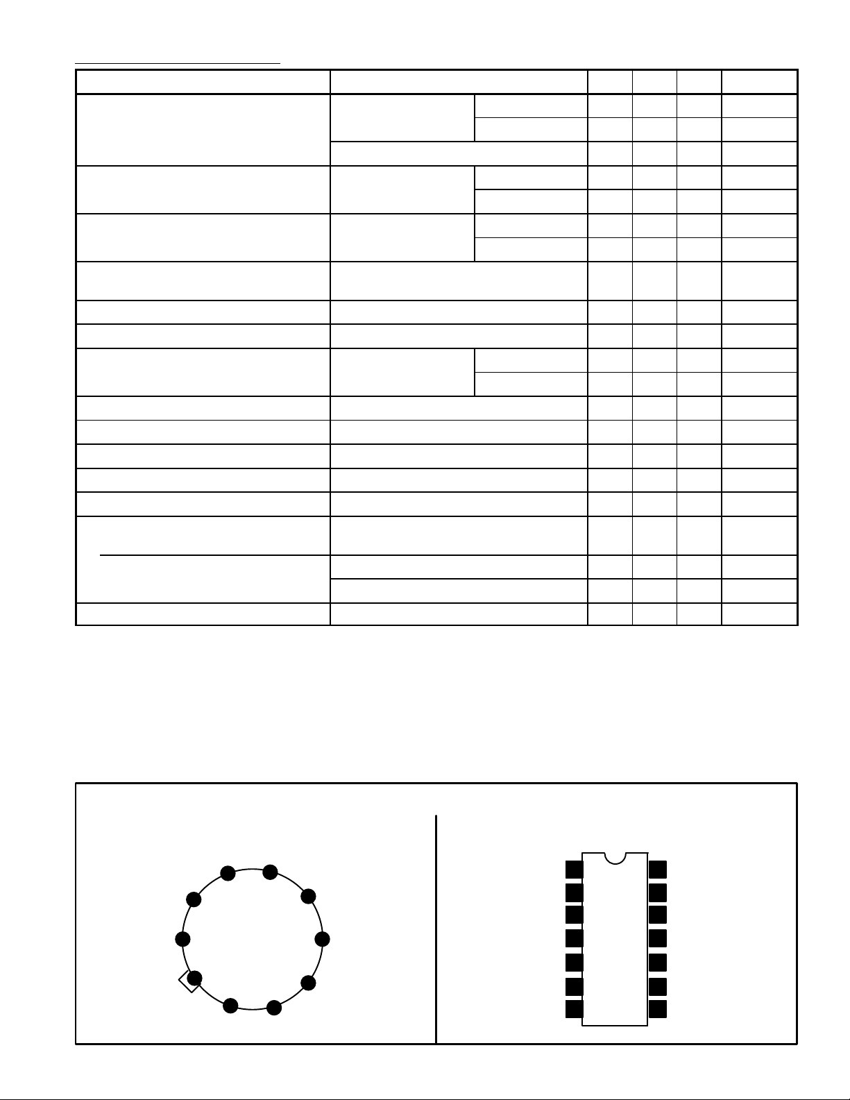
NTE923
(Top View)
V
C
7
V (+)
8
Freq Comp
Current Limit
9
10
1
Current Sense
V
6
2
Invert Input
.
OUT
out
V (–)/Case
5
4
3
Non–Invert Input
Pin Connection Diagram
V
ref
is required, an external 6.2V zener diode should be c on-
Z
NTE923D
N.C.
Current Limit
Current Sense
Invert Input
Non–Invert Input
V (–)
1
2
3
4
5
V
ref
6
7
14
13
12
11
10
V
V
V
9
8
N.C.
Freq Comp
V (+)
C
out
Z
N.C.
= 5V,
 Loading...