

NTE NTE922SM, NTE922 Datasheet
NTE922, NTE922M, & NTE922SM
Integrated Circuit
Voltage Comparator
Description:
The NTE922, NTE922M, and NTE922SM are voltage comparators that have input currents nearly
a thousand times lower than devices like the NTE910 or NTE910D. They are also designed to operate
over a wider range of supply voltages: from standard ±15V op amp supplies down to the single 5V
supply used for IC logic. Their output is compatible with RTL, DTL and TTL as well as MOS circuits.
Further, they can drive lamps or relays, switching voltages up to 50V at currents as high as 50mA.
Both the input and the output of these devices can be isolated from system ground, and the output
can drive loads referred to ground, the positive supply or the negative supply. Offset balancing and
strobe capability are provided and outputs can be wire OR’ed. Although slower than the NTE910 and
NTE910D (200ns response time vs 40ns) the devices are also much less prone to spurious oscillations.
Features:
D Operates from single 5V supply
D Input current: 150nA max. over temperature
D Offset current: 20nA max. over temperature
D Differential input voltage range: ±30V
D Power consumption: 135mW at ± 15V
D Available in 3 Different Case Styles:
8–Lead Metal Can: NTE922
8–Lead Mini DIP: NTE922M
8–Lead SOIC (Surface Mount): NTE922SM
Absolute Maximum Ratings:
Total Supply Voltage (V84) 36V. . . . . . . . . . . . . . . . . . . . . . . . . . . . . . . . . . . . . . . . . . . . . . . . . . . . . . . . . .
Output to Negative Supply Voltage (V
Ground to Negative Supply Voltage (V
Differential Input Voltage ±30V. . . . . . . . . . . . . . . . . . . . . . . . . . . . . . . . . . . . . . . . . . . . . . . . . . . . . . . . . . .
Input Voltage (Note 1) ±15V. . . . . . . . . . . . . . . . . . . . . . . . . . . . . . . . . . . . . . . . . . . . . . . . . . . . . . . . . . . . .
Power Dissipation (Note 2) 500mW. . . . . . . . . . . . . . . . . . . . . . . . . . . . . . . . . . . . . . . . . . . . . . . . . . . . . .
Note 1. This rating applied for ±15V supplies. The positive input voltage limit is 30V above the nega-
tive supply. The negative input voltage limit is equal to the negative supply voltage or 30V
below the positive supply, whichever is less.
Note 2. The maximum junction temperature is 110°C. For operating at elevated temperature, the
NTE922 must be derated based on a thermal resistance of 150°C/W, junction–to–ambient,
or 45°C/W, junction–to–case. The thermal resistance of the NTE922M and the NTE922SM
is 100°C/W, junction–to–ambient.
) 40V. . . . . . . . . . . . . . . . . . . . . . . . . . . . . . . . . . . . . . . . . . . . . .
74
) 30V. . . . . . . . . . . . . . . . . . . . . . . . . . . . . . . . . . . . . . . . . . . . .
14
Absolute Maximum Ratings (Cont’d):
Output Short Circuit Duration 10sec. . . . . . . . . . . . . . . . . . . . . . . . . . . . . . . . . . . . . . . . . . . . . . . . . . . . . .
Operating Temperature Range 0° to +70°C. . . . . . . . . . . . . . . . . . . . . . . . . . . . . . . . . . . . . . . . . . . . . . .
Storage Temperature Range –65° to +150°C. . . . . . . . . . . . . . . . . . . . . . . . . . . . . . . . . . . . . . . . . . . . . .
Lead Temperature (During Soldering, 10 sec) +260°C. . . . . . . . . . . . . . . . . . . . . . . . . . . . . . . . . . . . . .
Voltage at Strobe Pin V+ –5V. . . . . . . . . . . . . . . . . . . . . . . . . . . . . . . . . . . . . . . . . . . . . . . . . . . . . . . . . . . .
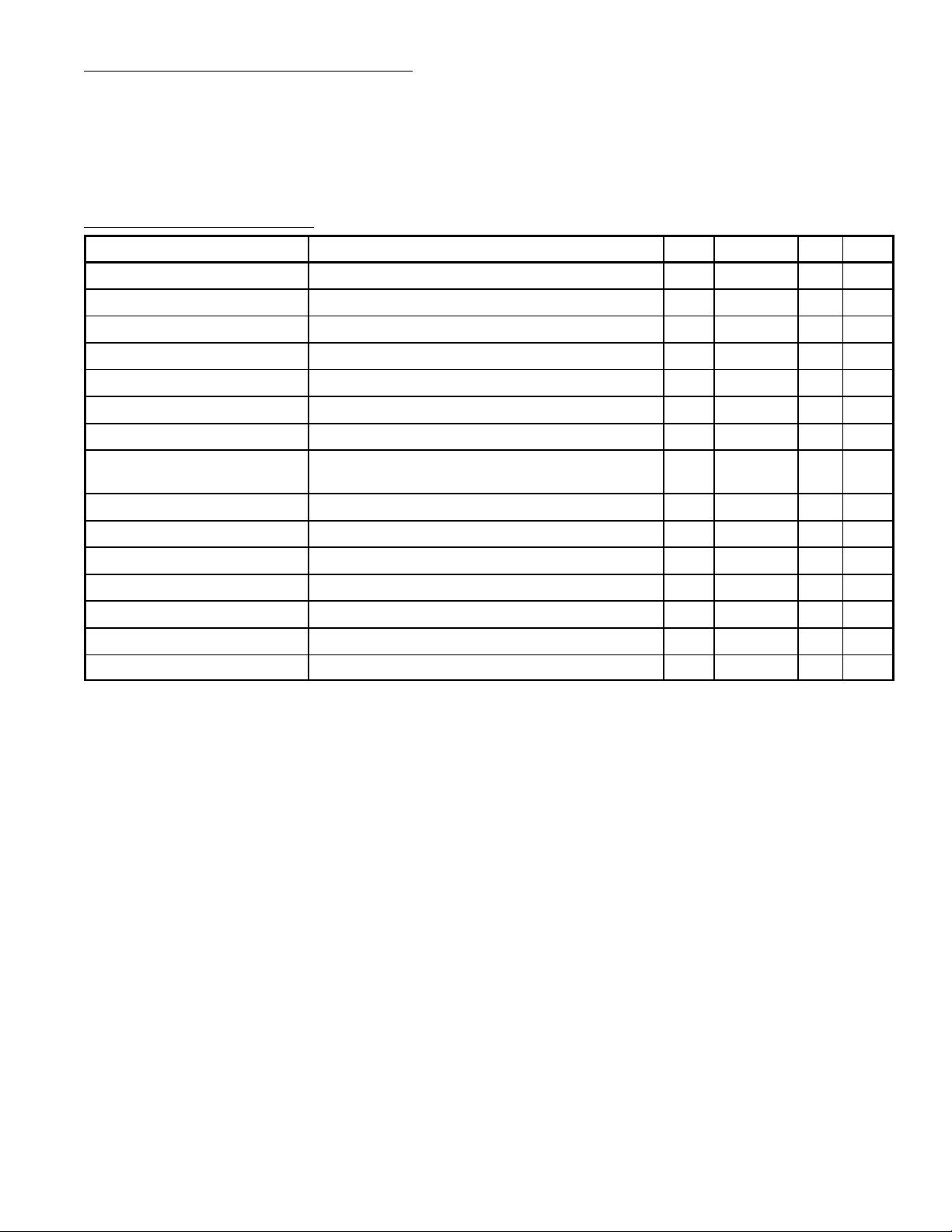
Electrical Characteristics:
Parameter Test Conditions Min Typ Max Unit
Input Offset Voltage TA = +25°C, RS ≤ 50k, Note 4 – 2.0 7.5 mV
Input Offset Current TA = +25°C, Note 4 – 6.0 50 nA
Input Bias Current TA = +25°C – 100 250 nA
Voltage Gain TA = +25°C 40 200 – V/mV
Response Time TA = +25°C, Note 5 – 200 – ns
Saturation Voltage VIN ≤ –10mV, I
Strobe ON Current TA = +25°C 1.5 3.0 – mA
Output Leakage Current VIN ≥ 10mV, V
Input Offset Voltage RS ≤ 50K, Note 4 – – 10 mV
Input Offset Current Note 4 – – 70 nA
Input Bias Current – – 300 nA
Input Voltage Range –14.5 13.8,–14.7 13.0 V
Saturation Voltage V+ ≥ 4.5V, V– = 0, VIN ≤ –10mV, I
Positive Supply Current TA = +25°C – 5.1 7.5 mA
Negative Supply Current TA = +25°C – 4.1 5.0 mA
(Note 3)
I
STROBE
= 3mA, V– = V
= 50mA, TA = +25°C – 0.75 1.5 V
OUT
= 35V TA = +25°C,
OUT
GRND
= –5V
≤ 8mA – 0.23 0.4 V
SINK
– 0.2 59 nA
Note 3. These specifications apply for VS = ±15V and the Ground pin at GND, and 0°C < TA < +70°C,
unless otherwise specified. The offset voltage, offset current and bias current specifications
apply for any supply voltage from a single 5V supply up to ± 15V supplies.
Note 4. The offset voltages and offset currents given are the maximum values required to drive the
output within a volt of either supply with 1mA load. Thus, these parameters define an error
band and take into account the worst–case effects of voltage gain and input impedance.
Note 5. Do not short the strobe pin to ground: it should be current driven at 3 to 5mA.
 Loading...