

NTE NTE919D Datasheet

NTE919D
Integrated Circuit
High Speed Dual Comparator
Description:
The NTE919D is a precision high speed dual comparator fabricated on a single monolithic chip. This
devices is designed to operate over a wide range of supply voltages down to a single 5V logic supply
and ground. Further, it has higher gain and lower input currents than devices like the NTE910. The
uncommitted collector of the output stage makes it compatible with RTL, DTL, and TTL as well as
capable of driving lamps and relays at currents up to 25mA.
Although designed primarily for applications requiring operation from digital logic supplies, the
NTE919D is fully specified for power supplies up to ±15V.
Features:
D Two Independent Comparators
D Operates from a Single 5V Supply
D Typically 80ns Response Time at ±15V
D Minimum Fan–Out of 2 Each Side
D Maximum Input Current of 1µA Over Temperature
D Inputs and Outputs can be Isolated from System Ground
D High Common Mode Slew Rate
Absolute Maximum Ratings:
Total Supply Voltage 36V. . . . . . . . . . . . . . . . . . . . . . . . . . . . . . . . . . . . . . . . . . . . . . . . . . . . . . . . . . . . . . . .
Output to Negative Supply Voltage 36V. . . . . . . . . . . . . . . . . . . . . . . . . . . . . . . . . . . . . . . . . . . . . . . . . . .
Ground to Negative Supply Voltage 25V. . . . . . . . . . . . . . . . . . . . . . . . . . . . . . . . . . . . . . . . . . . . . . . . . . .
Ground to Positive Supply Voltage 18V. . . . . . . . . . . . . . . . . . . . . . . . . . . . . . . . . . . . . . . . . . . . . . . . . . . .
Differential Input Voltage ±5V. . . . . . . . . . . . . . . . . . . . . . . . . . . . . . . . . . . . . . . . . . . . . . . . . . . . . . . . . . . .
Input Voltage (Note 1) ±15V. . . . . . . . . . . . . . . . . . . . . . . . . . . . . . . . . . . . . . . . . . . . . . . . . . . . . . . . . . . . . .
Power Dissipation (Note 2) 500mW. . . . . . . . . . . . . . . . . . . . . . . . . . . . . . . . . . . . . . . . . . . . . . . . . . . . . .
Output Short Circuit Duration 10sec. . . . . . . . . . . . . . . . . . . . . . . . . . . . . . . . . . . . . . . . . . . . . . . . . . . . . .
Operating Temperature Range 0° to +70°C. . . . . . . . . . . . . . . . . . . . . . . . . . . . . . . . . . . . . . . . . . . . . . . .
Storage Temperature Range –65° to +150°C. . . . . . . . . . . . . . . . . . . . . . . . . . . . . . . . . . . . . . . . . . . . . . .
Lead Temperature (Soldering 10 sec) +260°C. . . . . . . . . . . . . . . . . . . . . . . . . . . . . . . . . . . . . . . . . . . . . .
Note 1. For supply voltages less than ±15 the absolute maximum input voltage is equal to the supply
voltage.
Note 2. The maximum junction temperature is 85°C. For operating at elevated temperatures, de-
vices must be derated based on a thermal resistance of 100°C/W, junction to ambient.
Electrical Characteristics: (Note 3)
Parameter Test Conditions Min Typ Max Unit
Input Offset Voltage TA = +25°C, RS ≤ 5k, Note 4 – 2.0 8.0 mV
Input Offset Current TA = +25°C, Note 4 – 80 200 nA
Input Bias Current TA = +25°C – 250 1000 nA
Voltage Gain TA = +25°C, Note 6 8 40 – V/mV
Response Time TA = +25°C, VS = ±15V, Note 5 – 80 – ns
Saturation Voltage VIN ≤ –10mV, I
Output Leakage Current VIN ≥ 10mV, V
= +25°C
T
A
= 25mA TA = +25°C – 0.75 1.5 V
OUT
= 35V, V– = V
OUT
GND
= 0V,
– 0.2 10 µA
Input Offset Voltage RS ≤ 5k, Note 4 – – 10 mV
Input Offset Current Note 4 – – 300 nA
Input Bias Curent – – 1200 nA
Input Voltage Range VS = ±15V – ±13 – V
V+ = 5V, V– = 0 1 – 3 V
Saturation Voltage V+ ≥ 4.5V, V– = 0, VIN ≤ –10mV, I
≤ 3.2mA – 0.3 0.4 V
SINK
Differential Input Voltage – – ±5 V
Positive Supply Current TA = +25°C, V+ = 5V, V– = 0 – 4.3 – mA
Positive Supply Current TA = +25°C, VS = ±15V – 8 12.5 mA
Negative Supply Current TA = +25°C, VS = ±15V – 3 5 mA
Note 3. These specifications apply for VS = ±15V, and 0°C ≤ TA ≤ 70°C, unless otherwise stated.
The offset voltage, offset current and bias current specifications apply for any supply voltage
from a single 5V supply up to ±15V supplies. Do not operate the device with more than 16V
from ground to V
.
S
Note 4. The offset voltages and offset currents given are the maximum values required to drive the
output within a volt of either supply with a 1mA load. Thus, these parameters define an error
band and take into account the worst case effects of voltage gain and input impedance.
Note 5. The response time specified is for a 100mV input step with 5mV overdrive.
Note 6. Output is pulled up to 15V through a 1.4Ω resistor.
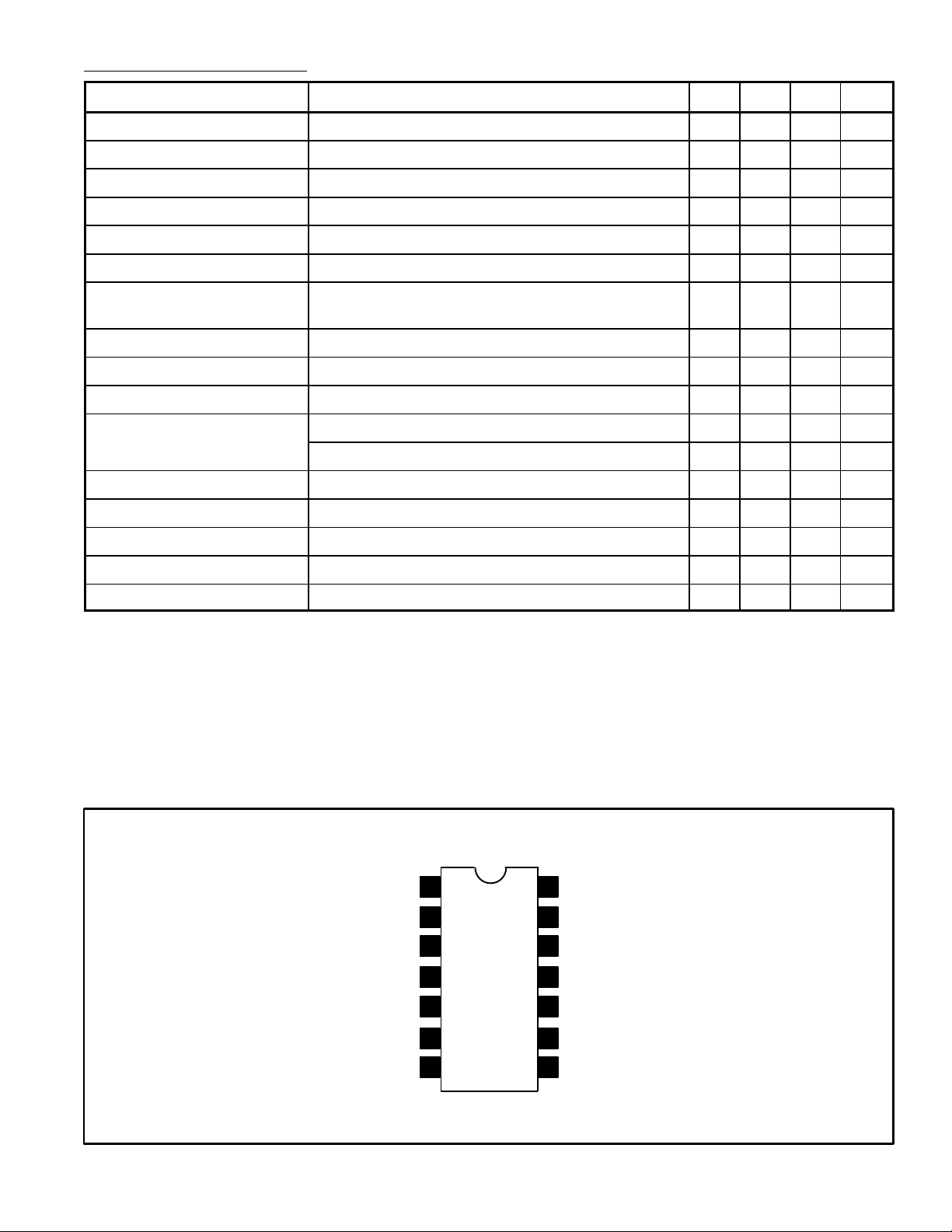
Pin Connection Diagram
N.C.
N.C.
GND 1
Non–Inverting Input 1
Inverting Input 1
V (–)
Output 2
1
2
3
4
5
6
7
N.C.
14
N.C.
13
Output 1
12
V (+)
11
Inverting Input 2
10
Non–Inverting Input 2
9
GND 2
8
 Loading...