

NTE NTE916 Datasheet
NTE916
Integrated Circuit
High Current, NPN Transistor Array,
Common Emitter
Description:
The NTE916 i s a high c urrent transistor array in a 1 6–Lead DIP type package consisting of seven
silicon N PN t ransistors on a common m onolithic s ubstrate connected i n a c ommon–emitter c onfig uration designed for directly driving s even–segment displays a nd light–emitting diodes (LED) d is plays. This d evice is a lso well suited f or a v ariety of o t her d rive applications i ncluding relay c ontrol
and thyristor firing.
Features:
D Seven Transistors Permit a Wide Range of Applications
D High Collector Current: I
D Low Collector–Emitter Saturation Voltage: V
= 100mA Max
C
CE(sat)
= 400mV Typ @ 50mA
Absolute Maximum Ratings:
Power Dissipation (Total Package), P
(TA = +25°C unless otherwise specified)
D
750mW. . . . . . . . . . . . . . . . . . . . . . . . . . . . . . . . . . . . . . . . . . . .
Per Transistor 500mW. . . . . . . . . . . . . . . . . . . . . . . . . . . . . . . . . . . . . . . . . . . . . . . . . . . . . . . . . . . .
Derate Linearly Above 55°C 6.67mW/°C. . . . . . . . . . . . . . . . . . . . . . . . . . . . . . . . . . . . . . . . .
Operating Ambient Temperature Range, T
Storage Temperature Range, T
stg
A
Lead Temperature (During Soldering, 1/16” from case, 10sec max), T
L
–55° to +125°C. . . . . . . . . . . . . . . . . . . . . . . . . . . . . . . . . .
–65° to +150°C. . . . . . . . . . . . . . . . . . . . . . . . . . . . . . . . . . . . . . . . . .
+265°C. . . . . . . . . . . . . . . . .
The Following Ratings Apply for Each Transistor in the Device
Collector–Emitter Voltage, V
Collector–Base Voltage, V
CEO
CBO
Collector–Substrate Voltage (Note 1), V
Emitter–Base Voltage, V
Collector Current, I
Base Current, I
B
EBO
C
CIO
16V. . . . . . . . . . . . . . . . . . . . . . . . . . . . . . . . . . . . . . . . . . . . . . . . . . . . . .
20V. . . . . . . . . . . . . . . . . . . . . . . . . . . . . . . . . . . . . . . . . . . . . . . . . . . . . . .
20V. . . . . . . . . . . . . . . . . . . . . . . . . . . . . . . . . . . . . . . . . . . .
5V. . . . . . . . . . . . . . . . . . . . . . . . . . . . . . . . . . . . . . . . . . . . . . . . . . . . . . . . . .
100mA. . . . . . . . . . . . . . . . . . . . . . . . . . . . . . . . . . . . . . . . . . . . . . . . . . . . . . . . . . . . .
20mA. . . . . . . . . . . . . . . . . . . . . . . . . . . . . . . . . . . . . . . . . . . . . . . . . . . . . . . . . . . . . . . . .
Note 1. The collector of each transistor of the NTE916 is isolated from the substrate by an integral
diode. The substrate must be connected to a voltage which is more negative that any collector voltage in order to maintain isolation between transistors and provide normal transistor
action. To avoid undesired coupling between transistors, the substrate terminal (Pin5)
should be maintained at either DC or signal (AC) ground. A suitable bypass capacitor can
be used to establish a signal ground.
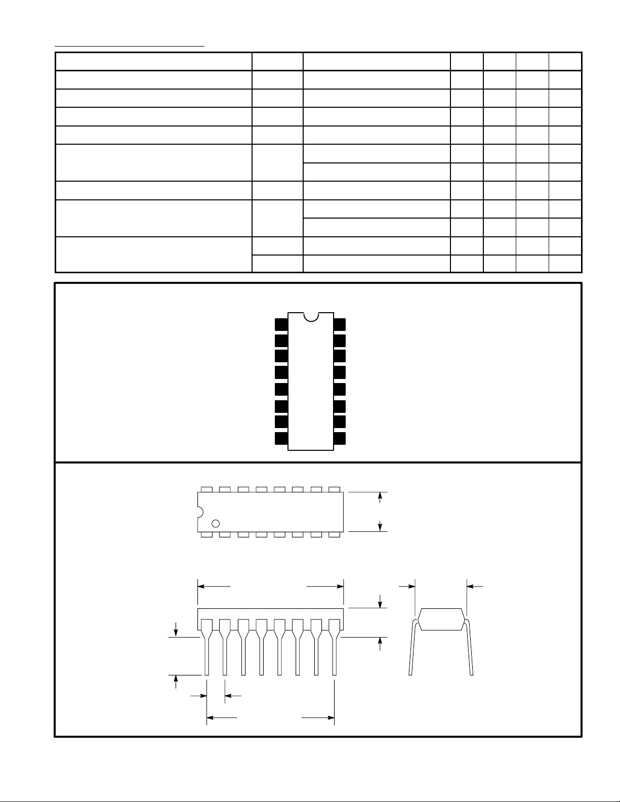
Electrical Characteristics: (TA = +25°C unless otherwise specified)
Parameter Symbol Test Conditions Min Typ Max Unit
Collector–Base Breakdown Voltage V
Collector–Substrate Breakdown Voltage V
Collector–Emitter Breakdown Voltage V
Emitter–Base Breakdown Voltage V
(BR)CESIC
(BR)CIOICI
(BR)CEOIC
(BR)EBOIC
DC Forward Current Transfer Ratio h
Base–Emitter Saturation Voltage V
Collector–Emitter Saturation Voltage V
BE(sat)IC
CE(sat)IC
Collector Cutoff Current I
I
Pin Connection Diagram
Collector Q11
Collector Q
Base Q
Collector Q
Base Q
Collector Q
Base Q
FE
CEO
CBO
2
2
5
5
7
7
= 500µA, IE = 0 20 60 – V
= 500µA, IE = 0, IB = 0 20 60 – V
= 1mA, IB = 0 16 24 – V
= 500µA 5.0 6.9 – V
VCE = 500mV, IC = 30mA 30 68 –
VCE = 800mV, IC = 50mA 40 70 –
= 30mA, IB = 1mA – 0.87 1.0 V
= 30mA, IB = 1mA – 0.27 0.5 V
IC = 50mA, IB = 5mA – 0.4 0.7 V
VCE = 10V, IB = 0 – – 10 µA
VCB = 10V, IE = 0 – – 1 µA
Base Q
16
2
3
4
5Substrate
6
7
8
15
Common Emitter
Collector Q
14
Base Q
13
Collector Q
12
Base Q
11
Base Q
10
Collector Q
9
1
3
3
4
4
6
6
.245
(6.22)
Min
16 9
.260 (6.6) Max
18
.785 (19.9)
Max
.300
(7.62)
.200 (5.08)
Max
.100 (2.54)
.700 (17.7)
 Loading...