

NTE NTE912 Datasheet

NTE912
Integrated Circuit
General Purpose Transistor Array
(Three Isolated Transistors and One Differentially–Connected Transistor Pair)
Description:
The NTE912 consists of five general–purpose silicon NPN transistors on a common monolithic substrate in a 14–Lead DIP type package. Two of the transistors are internally connected to form a differentially–connected pair.
The transistors of the NTE912 are well suited to a wide variety of applications in low power systems
in the DC through VHF range. They may be used as discrete transistors in conventional circuits. However, i n addition, they provide the very significant inherent integrated circuit advantages of close electrical and thermal matching.
Features:
D Two Matched Pairs of Transistors:
matched ±5mV
V
BE
Input Offset Current 2µA Max. @ I
D 5 General Purpose Monolithic Transistors
D Operation from DC to 120MHz
D Wide Operating Current Range
D Low Noise Figure: 3.2dB Typ @ 1kHz
= 1mA
C
Applications:
D General Use In All Types of Signal Processing Systems Operating Anywhere in the Frequency
Range from DC to VHF
D Custom Designed Differential Amplifiers
D Temperature Compensated Amplifiers
Absolute Maximum Ratings:
Power Dissipation (T
≤ +55°C), P
A
(TA = +25°C unless otherwise specified)
D
Each Transistor 300mW. . . . . . . . . . . . . . . . . . . . . . . . . . . . . . . . . . . . . . . . . . . . . . . . . . . . . . . . . .
Total Package 750mW. . . . . . . . . . . . . . . . . . . . . . . . . . . . . . . . . . . . . . . . . . . . . . . . . . . . . . . . . . .
Derate Above 55°C 6.67mW/°C. . . . . . . . . . . . . . . . . . . . . . . . . . . . . . . . . . . . . . . . . . . . . . . . .
Collector Emitter Voltage, V
Collector Base Voltage, V
Collector Substrate Voltage (Note 1), V
Emitter Base Voltage, V
Collector Current, I
C
Operating Temperature Range, T
Storage Temperature Range, T
CEO
CBO
CIO
EBO
opr
stg
Lead Temperature (During Soldering, 1/16” ±1/32” from case, 10sec max), T
–55° to +125°C. . . . . . . . . . . . . . . . . . . . . . . . . . . . . . . . . . . . . . . .
–65° to +150°C. . . . . . . . . . . . . . . . . . . . . . . . . . . . . . . . . . . . . . . . . .
L
15V. . . . . . . . . . . . . . . . . . . . . . . . . . . . . . . . . . . . . . . . . . . . . . . . . . . . . .
20V. . . . . . . . . . . . . . . . . . . . . . . . . . . . . . . . . . . . . . . . . . . . . . . . . . . . . . . .
20V. . . . . . . . . . . . . . . . . . . . . . . . . . . . . . . . . . . . . . . . . . . . .
5V. . . . . . . . . . . . . . . . . . . . . . . . . . . . . . . . . . . . . . . . . . . . . . . . . . . . . . . . . . .
50mA. . . . . . . . . . . . . . . . . . . . . . . . . . . . . . . . . . . . . . . . . . . . . . . . . . . . . . . . . . . . . .
+265°C. . . . . . . . . . .
Note 1. The collector of each transistor is isolated from the substrate by an integral diode. The sub-
strate (Pin13) must be connected to the most negative point in the external circuit to maintain
isolation between transistors and to provide for normal transistor action.
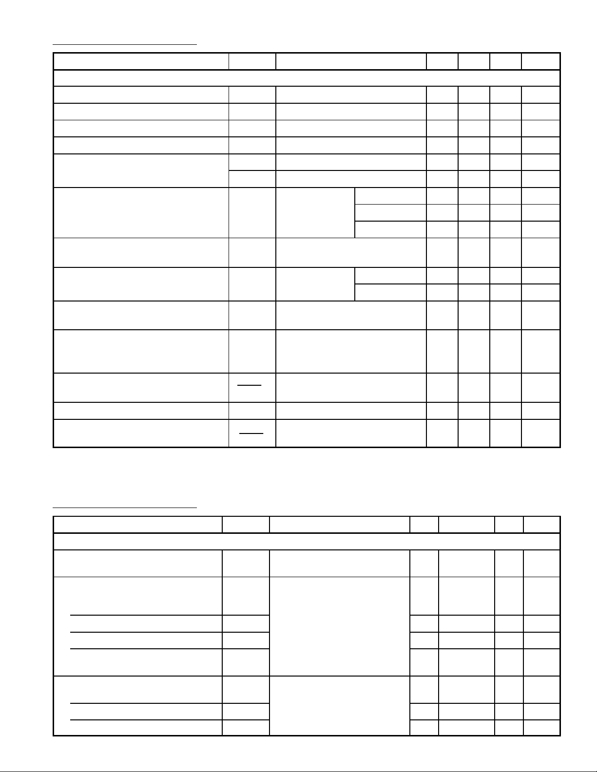
Electrical Characteristics: (TA = +25°C unless otherwise specified)
Parameter Symbol Test Conditions Min Typ Max Unit
Static Characteristics
Collector Base Breakdown Voltage V
Collector Emitter Breakdown Voltage V
Collector Substrate Breakdown Voltage V
Emitter Base Breakdown Voltage V
(BR)CBOIC
(BR)CEOIC
(BR)CIOIC
(BR)EBOIE
Collector Cutoff Current I
Static Forward Current Transfer Ratio h
Input Offset Current for Matched Pair
– I
and Q2.
Q
1
|I
IO
|
IO
1
2
Base Emitter Voltage V
Magnitude of Input Offset Voltage for
– V
Differential Pair
|V
BE
1
BE
|
2
Magnitude of Input Offset Voltage for
– V
|
BE
4
||V
3
∆V
|V
BE
5
|V
BE
– V
3
BE
Isolated Transistors
– V
BE
|
5
BE
4
Temperature Coefficient of Base Emitter
Voltage
Collector Emitter Saturation Voltage V
Temperature Coefficient:
|∆VIO|∆TVCE = 3V, IC = 1mA – 1.1 – µV/°C
Magnitude of Input–Offset Voltage
CBO
I
CEO
FE
BE
BE
∆T
CESIB
= 10µA, IE = 0 20 60 – V
= 1mA, IB = 0 15 24 – V
= 10µA, ICI = 0 20 60 – V
= 10µA, IC = 0 5 7 – V
VCB = 10V, IE = 0 – 0.002 40 nA
VCE = 10V, IB = 0 – – 0.5 µA
VCE = 3V IC = 10mA – 100 –
IC = 1mA 40 100 –
IC = 10µA – 54 –
VCE = 3V, IC = 1mA – 0.3 2.0 µA
VCE = 3V IE = 1mA – 0.715 – V
IE = 10mA – 0.800 – V
VCE = 3V, IC = 1mA – 0.45 5.0 mV
VCE = 3V, IC = 1mA – 0.45 5.0 mV
VCE = 3V, IC = 1mA – –1.9 – mV/°C
= 1mA, IC = 10mA – 0.23 – V
Electrical Characteristics: (TA = +25°C unless otherwise specified)
Parameter Symbol Test Conditions Min Typ Max Unit
Dynamic Characteristics
Low–Frequency Noise Figure NF f = 1kHz, VCE = 3V, IC = 100µA,
Source Resistance = 1kΩ
Low–Frequency, Small–Signal
Equivalent Circuit Characteristics:
Forward Current Transfer Ratio
Short–Circuit Input Impedance h
Open–Circuit Output Impedance h
Open–Circuit Reverse Voltage
Transfer Ratio
Admittance Characteristics:
Forward Transfer Admittance
Input Admittance Y
Output Admittance Y
h
h
Y
f = 1kHz, VCE = 3V, IC = 1mA
fe
ie
oe
re
f = 1kHz, VCE = 3V, IC = 1mA – 31–j1.5 –
fe
ie
oe
– 3.25 – dB
– 110 –
– 3.5 – kΩ
– 15.6 – µmhos
– 1.8x10
–4
–
– 0.3+j0.04 –
– 0.001+j0.03 –
 Loading...