

NTE NTE909D, NTE909 Datasheet
NTE909 & NTE909D
Integrated Circuits
Operational Amplifier
Description:
These devices are monolithic operational amplifiers intended for general–purpose applications. Operation is completely specified over the range of voltages commonly used for these devices. The design, in addition to providing high gain, minimizes both offset voltages and bias currents. Further, the
class–B output stage gives a large output capability with minimum power drain.
External components are used to frequency compensate the amplifier . Although the unity–gain compensation network specified will make the amplifiers unconditionally stable in all feedback configurations, compensation can be tailored to optimize high–frequency performance for any gain setting.
The fact that the amplifiers are built on a single silicon chip provides low offset and temperature drift
at minimum cost. It also ensures negligble drift due to temperature gradients in the vicinity of the amplifier.
Absolute Maximum Ratings:
Supply Voltage ±18V. . . . . . . . . . . . . . . . . . . . . . . . . . . . . . . . . . . . . . . . . . . . . . . . . . . . . . . . . . . . . . . . . . .
Power Dissipation (Note 1) 250mW. . . . . . . . . . . . . . . . . . . . . . . . . . . . . . . . . . . . . . . . . . . . . . . . . . . . . .
Differential Input Voltage ±10V. . . . . . . . . . . . . . . . . . . . . . . . . . . . . . . . . . . . . . . . . . . . . . . . . . . . . . . . . . .
Input Voltage ±10V. . . . . . . . . . . . . . . . . . . . . . . . . . . . . . . . . . . . . . . . . . . . . . . . . . . . . . . . . . . . . . . . . . . . .
Output Short–Circuit Duration (T
Storage Temperature Range –65° to +150°C. . . . . . . . . . . . . . . . . . . . . . . . . . . . . . . . . . . . . . . . . . . . . .
Operating Temperature Range 0° to +70°C. . . . . . . . . . . . . . . . . . . . . . . . . . . . . . . . . . . . . . . . . . . . . . .
Lead Temperature (Soldering, 10 seconds) +300°C. . . . . . . . . . . . . . . . . . . . . . . . . . . . . . . . . . . . . . . .
= +25°C) 5 seconds. . . . . . . . . . . . . . . . . . . . . . . . . . . . . . . . . . . . . .
A
Note 1 For operating at elevated temperatures, the device must be derated based on a 100°C maxi-
mum junction temperature and a thermal resistance 150°C/W junction to ambient or 45°C/W,
junction to case for the metal can package.
Electrical Characteristics:
(0°C ≤ TA = ≤ +70°C, ±9V ≤ VS ≤ ±15V, C1 = 5000pF, R1 = 1.5k,
C2 = 200pF and R2 = 51Ω unless otherwise specified)
Parameter Test Conditions Min Typ Max Unit
Input Offset Voltage TA = +25°C, RS ≤ 10kΩ – 2.0 7.5 mV
Input Bias Current TA = +25°C – 300 1500 nA
TA = T
Input Offset Current TA = +25°C – 100 500 nA
TA = T
TA = T
MIN
MIN
MAX
– 0.36 2.0 µA
– 75 400 nA
– 125 750 nA
Electrical Characteristics (Cont’d): (0°C ≤ TA = ≤ +70°C, ±9V ≤ VS ≤ ±15V, C1 = 5000pF,
R1 = 1.5k, C2 = 200pF and R2 = 51Ω unless otherwise
specified)
Parameter Test Conditions Min Typ Max Unit
Input Resistance TA = +25°C 50 250 – kΩ
TA = T
MIN
50 250 – kΩ
Output Resistance TA = +25°C – 150 – Ω
Supply Current TA = +25°C, VS = ±15V – 2.6 6.6 mA
Transient Response Risetime VIN = 20mV, CL ≤ 100pF, TA = +25°C – 0.3 1.0 µs
Transient Response Overshoot – 10 30 %
Slew Rate TA = +25°C – 0.25 – V/µs
Average Temperature Coefficient
of Input Offset Voltage
RS = 50Ω, TA = +25°C to T
RS = 50Ω, TA = +25°C to T
Large Signal Voltage VS = ±15V, RL ≥ 2kΩ, V
MAX
MIN
= ±10V 15 45 – V/mV
OUT
– 6.0 – µV/°C
– 12 – µV/°C
Output Voltage Swing VS = ±15V, RL = 10kΩ ±12 ±14 – V
VS = ±15V, RL = 2kΩ ±10 ±13 – V
Input Voltage Range VS = ±15V ±8 ±10 – V
Common Mode Rejection Ratio RS ≥ 10kΩ 65 90 – dB
Supply Voltage Rejection Ratio RS ≥ 10kΩ – 25 200 µV/V
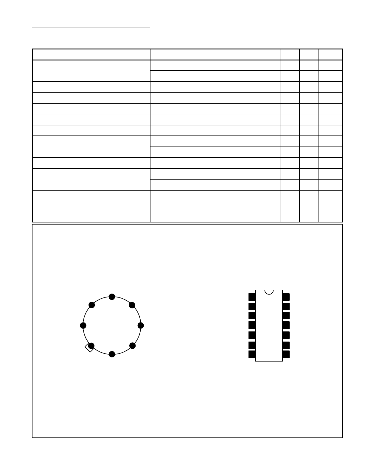
Pin Connection Diagram
Output
V (+)
Input Freq Comp B
NTE909
(Top View)
Output Freq Comp
6
7
8
Input Freq Comp A
NTE909D
5
1
V (–)
4
3
Non–Invert Input
2
Invert Input
Input Freq Comp A
N.C.
N.C.
Invert Input
1
2
3
4
5Non–Invert Input
6V (–)
7N.C.
N.C.
14
N.C.
13
Input Freq Comp B
12
11
V (+)
10 Output
Output Freq Comp
9
8 N.C.
 Loading...