

NTE NTE9093, NTE9094 Datasheet
NTE9093 & NTE9094
Integrated Circuit
Diode Transistor Logic (DTL)
Dual J–K Flip–Flop
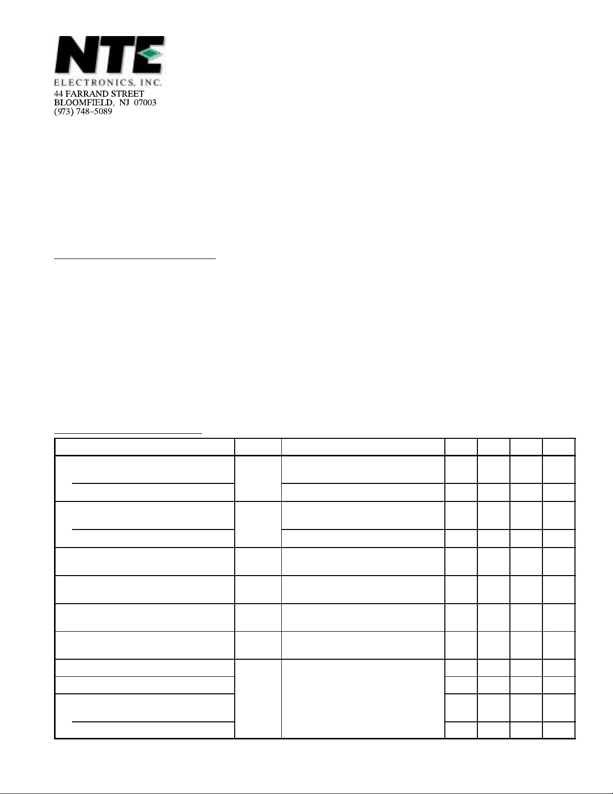
Absolute Maximum Ratings: (Above which useful life may be impaired)
VCC Pin, Potential to GND –0.5 to +8.0V. . . . . . . . . . . . . . . . . . . . . . . . . . . . . . . . . . . . . . . . . . . . . . . . . .
VCC, Pulsed, 1 Second 12V. . . . . . . . . . . . . . . . . . . . . . . . . . . . . . . . . . . . . . . . . . . . . . . . . . . . . . . . . . . . . .
Input Voltage, Applied to Input –1.5 to 5.5V. . . . . . . . . . . . . . . . . . . . . . . . . . . . . . . . . . . . . . . . . . . . . . . .
Voltage Applied to Output when Output is High +V
Input Current, Into Inputs 1mA. . . . . . . . . . . . . . . . . . . . . . . . . . . . . . . . . . . . . . . . . . . . . . . . . . . . . . . . . . .
Current Into Output when Output is Low 30mA. . . . . . . . . . . . . . . . . . . . . . . . . . . . . . . . . . . . . . . . . . . . .
Ambient Temperature Range Under Bias –55° to +125°C. . . . . . . . . . . . . . . . . . . . . . . . . . . . . . . . . . . .
Storage Temperature Range –65° to +150°C. . . . . . . . . . . . . . . . . . . . . . . . . . . . . . . . . . . . . . . . . . . . . . .
Lead Temperature (During Soldering, 60sec) +300°C. . . . . . . . . . . . . . . . . . . . . . . . . . . . . . . . . . . . . . .
Note 1. The NTE9093 is a discontinued device and no longer available.
Electrical Characteristics: (TA = +25°C, VCC = 5V ±10% unless otherwise specified)
Parameter Symbol Test Conditions Min Typ Max Unit
. . . . . . . . . . . . . . . . . . . . . . . . . . . . . . . . . . . . . . . .
CC
Output High Voltage
NTE9093
NTE9094 VCC = 4.5V, IOH = –540µA 2.5 3.3 – V
Output Low Voltage
NTE9093
NTE9094 VCC = 4.5V, IOH = 13mA – 0.25 0.4 V
Input High Voltage V
Input Low Voltage V
Input Leakage Current,
All J–K, S, C, SD, CD Inputs
Input Leakage Current, CP Inputs I
Input Current, All J, K, S, C Inputs I
Input Current, SD or C
Input Current, CP Inputs
NTE9093
NTE9094 – –1.93 –2.35 mA
D
V
OH
V
OL
I
RCP
VCC = 4.5V, IOH = –180µA 2.5 3.3 – V
VCC = 4.5V, IOL = 12mA – 0.25 0.4 V
Guaranteed Input High Threshold
IH
for All Inputs
Guaranteed Input Low Threshold
IL
for All Inputs
VCC = 5.5V, VR = 4V, GND on
R
Other Inputs
VCC = 5.5V, VR = 4V, GND on
Other Inputs
VCC = 5.5V, VF = 0.4V,
F
4V on Other Inputs
1.9 – – V
– – 1.1 V
– – 2.0 µA
– – 10 µA
– –0.82 –0.98 mA
– –1.8 –2.2 mA
– –2.40 –2.93 mA
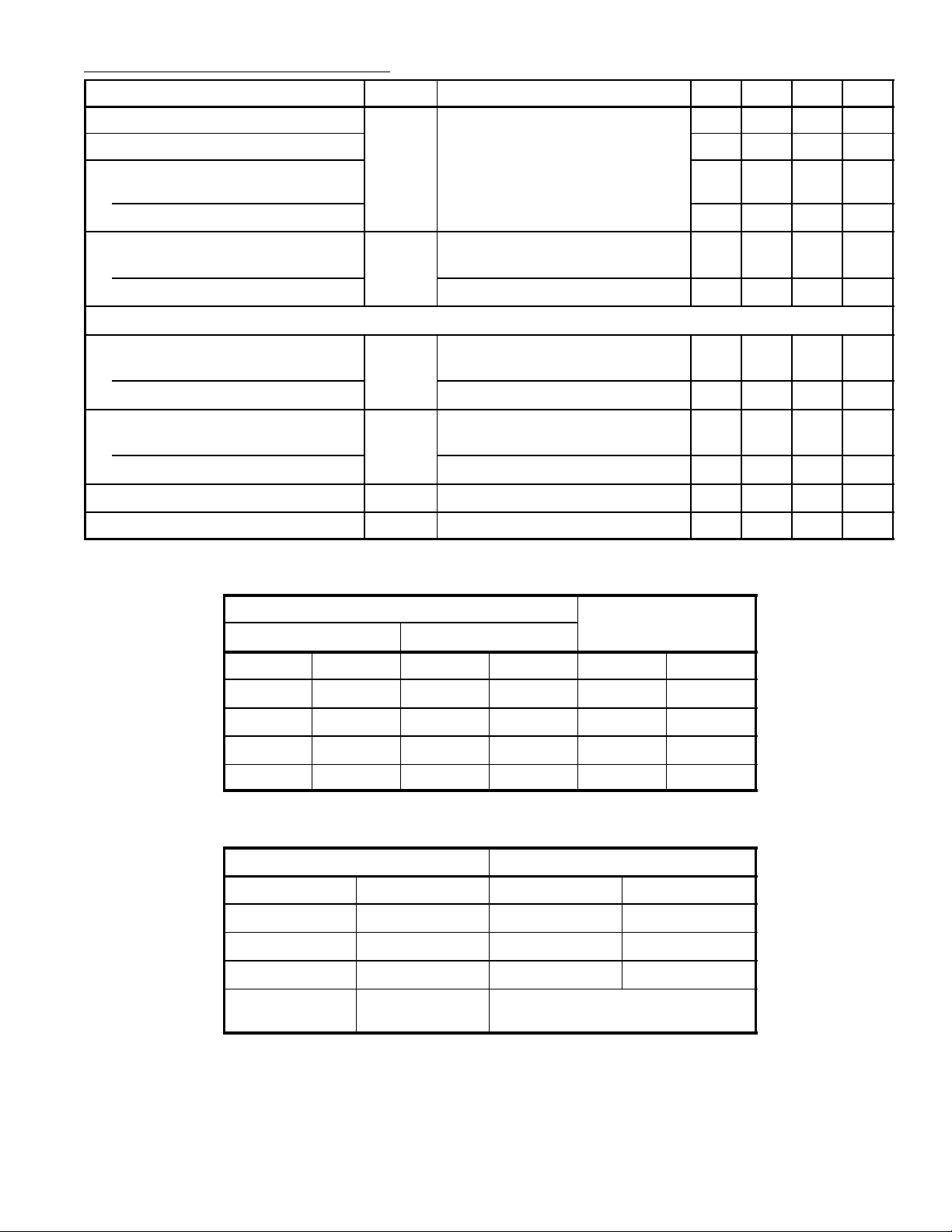
Electrical Characteristics (Cont’d): (TA = +25°C, VCC = 5V ±10% unless otherwise specified)
Parameter Symbol Test Conditions Min Typ Max Unit
Input Current, All J, K, S, C Inputs I
Input Current, SD or C
Input Current, CP Inputs
NTE9093
NTE9094 – –1.50 –1.83 mA
VCC Current
D
I
PD
NTE9093
NTE9094 – 19.8 32.4 mA
VCC = 4.5V, VF = 0.4V,
F
4V on Other Inputs
VCC = 5V, All Inputs Open,
Momentary GND on S
D
– –0.62 –0.76 mA
– –1.39 –1.70 mA
– –1.85 –2.26 mA
– 16.6 28.0 mA
Switching Characteristics (TA = +25°C, VCC = 5V)
Clock to Output
NTE9093
NTE9094 30 – 65 ns
Clock to Output
NTE9093
NTE9094 30 – 75 ns
Set–Up Time
Release Time
t
pd+
t
pd–
t
set–up
t
release
35 – 75 ns
30 – 75 ns
35 22 – ns
– 14 10 ns
Truth Table: Synchronous Operation
Before Clock
Outputs Inputs
One Zero J K One Zero
L H L X L H
L H H X H L
H L X L H L
H L X H L H
Outputs After
Outputs After
Clock
Truth Table: Asynchronous Operation
Inputs Outputs
S
D
L L H H
L H H L
H L L H
H H State determined by synchronous
C
D
One Zero
inputs and clock input
 Loading...