

NTE NTE907 Datasheet

NTE907
Integrated Circuit
Diode Array
Description:
The NTE907 consists of six ultra–fast, low capacitance diodes on a common monolithic substrate.
Five of the diodes are independently accessible, with the sixth sharing a common terminal with the
substrate. The NTE907 comes in a 12–Lead TO5 type package.
Features:
D Excellent Reverse Recovery Time: 1ns typ.
D Matched Monolithic Construction: V
D Low Diode Capacitance: C
= 0.65pF typical at VR = –2V
D
Applications:
D Balanced Modulators or Demodulators
D Ring Modulators
D High Speed Diode Gates
D Analog Switches
matched within 5mV
F
Absolute Maximum Ratings:
Power Dissipation, P
D
(TA = +25°C unless otherwise specified)
Any one diode unit 100mW. . . . . . . . . . . . . . . . . . . . . . . . . . . . . . . . . . . . . . . . . . . . . . . . . . . . . . .
Total for device 600mW. . . . . . . . . . . . . . . . . . . . . . . . . . . . . . . . . . . . . . . . . . . . . . . . . . . . . . . . . .
For T
Operating Temperature Range, T
Storage Temperature Range, T
Peak Inverse Voltage, P
> 55°C derate linearly 5.7mW/°C. . . . . . . . . . . . . . . . . . . . . . . . . . . . . . . . . . . . . . . . . . . .
A
opr
stg
IV
D1 – D5 5V. . . . . . . . . . . . . . . . . . . . . . . . . . . . . . . . . . . . . . . . . . . . . . . . . . . . . . . . . . . . . . . . . . . . . .
D
6
Peak Diode–to–Substrate Voltage, V
for D1–D5 (Pin1, 4, 5, 8, or 12 to Pin10) +20V, –1V. . . . . . . . . . . . . . . . . . . . . . . . . . . . . . . . . . .
DC Forward Current, I
Peak Recurrent Forward Current, I
Peak Forward Surge Current, I
Lead Temperature, T
25mA. . . . . . . . . . . . . . . . . . . . . . . . . . . . . . . . . . . . . . . . . . . . . . . . . . . . . . . . . . .
F
F
(Surge) 100mA. . . . . . . . . . . . . . . . . . . . . . . . . . . . . . . . . . . . . . . . . . .
F
L
(During soldering 1/16 ±1/32” (1.59 ± 0.79mm) from case for 10sec Max) +265°C. . . . . . . . .
–55° to +125°C. . . . . . . . . . . . . . . . . . . . . . . . . . . . . . . . . . . . . . . .
–65° to +150°C. . . . . . . . . . . . . . . . . . . . . . . . . . . . . . . . . . . . . . . . . .
0.5V. . . . . . . . . . . . . . . . . . . . . . . . . . . . . . . . . . . . . . . . . . . . . . . . . . . . . . . . . . . . . . . . . . . . . . . . .
DI
100mA. . . . . . . . . . . . . . . . . . . . . . . . . . . . . . . . . . . . . . . . . . . . . . .
Electrical Characteristics: (TA = +25°C, Note 1 unless otherwise specified)
Parameter Symbol Test Conditions Min Typ Max Unit
DC Forward Voltage Drop V
F
IF = 50µA – 0.65 0.69
V
IF =1 mA – 0.73 0.78
IF = 3mA – 0.76 0.80
IF = 10mA – 0.81 0.90
DC Reverse Breakdown Voltage V
DC Reverse Breakdown Voltage
(BR)R
V
(BR)R
IR = –10µA 5 7 – V
IR = –10µA 20 – – V
Between any Diode Unit and
Substrate
DC Reverse (Leakage) Current I
DC Reverse (Leakage) Current
R
I
R
VR = –4V – 0.016 100 nA
VR = –10V – 0.022 100 nA
Between any Diode Unit and
Substrate
Magnitude of Diode Offset Voltage
|VF1–VF2| IF = 1mA – 0.5 5 mV
(Difference in DC Forward Voltage
Drops of any Two Diode Units)
Temperature Coefficient of |VF1–VF2| ∆|VF1–VF2|∆TIF = 1mA – 1 – µV/°C
Temperature Coefficient of Forward
Drop
DC Forward Voltage Drop for
Anode–to–Substrate Diode (D
)
S
Reverse Recovery Time t
Diode Resistance R
Diode Capacitance C
Diode–to–Substrate Capacitance C
∆V
∆T
V
F
rr
D
D
D1
F
IF = 1mA – –1.9 – mV/°C
IF = 1mA – 0.65 – V
IF = 10mA, IR = 10mA – 1 – ns
f = 1kHz, IF = 1mA 25 30 45 Ω
VR = –2V, IF = 0 – 0.65 – pF
VD1 = +4V, IF = 0 – 3.2 – pF
Note 1. Characteristics apply for each diode unit, unless otherwise specified.
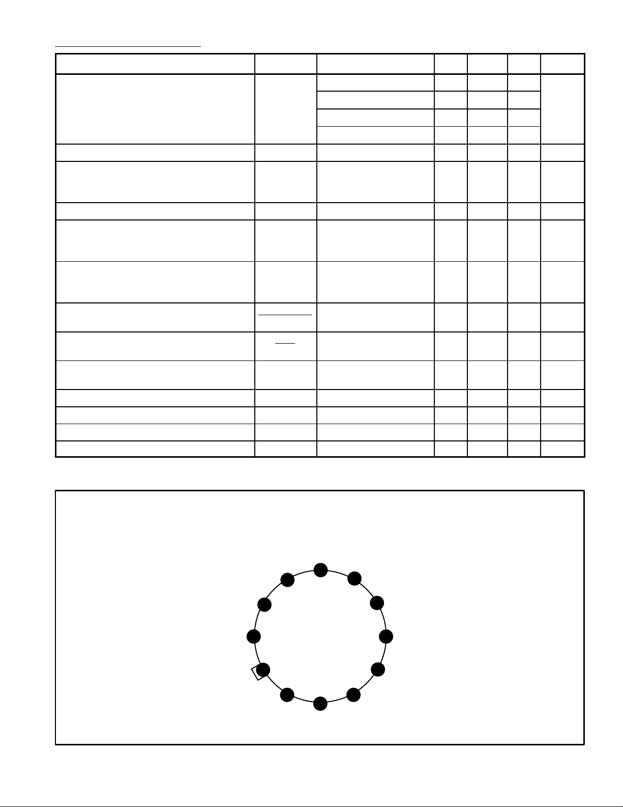
Anode D
Cathode D6/
Substrate & Case
Cathode D
Anode D
5
5
Anode D
Pin Connection Diagram
10
11
12
Anode D
9
6
1
4
(Top View)
1
8
1
2
Cathode D
6
Cathode D
7
Cathode D
3
4
6
Cathode D
5
Anode D
Anode D
4
1
2
2
3
3
 Loading...