

NTE NTE906 Datasheet

NTE906
Integrated Circuit
Dual, High Frequency, Differential Amplifier
Description:
The NTE906 is an integrated circuit in a 12–Lead TO5 type package consisting of two independent
differential amplifiers with associated constant–current transistors on a common monolithic substrate. The six transistors which comprise the amplifiers are general–purpose devices which exhibit
low 1/f noise and a value of f
to 500MHz. Bias and load resistors have been omitted to provide maximum application flexibility.
The monolithic construction of the NTE906 provides close electrical and thermal matching of the amplifiers. This feature makes this device particularly useful in dual–channel applications where
matched performance of the two channels is required.
Features:
D Power Gain: 23dB (Typ) @ 200MHz
D Noise Figure: 4.6dB (Typ) @ 200MHz
D Two Different Amplifiers on a Common Substrate
D Independently Accessible Input and Outputs
in excess of 1GHz. These features make the NTE906 useful from DC
T
Absolute Maximum Ratings:
Power Dissipation, P
D
(TA = +25°C unless otherwise specified)
Any One Transistor 300mW. . . . . . . . . . . . . . . . . . . . . . . . . . . . . . . . . . . . . . . . . . . . . . . . . . . . . . .
Total Package 600mW. . . . . . . . . . . . . . . . . . . . . . . . . . . . . . . . . . . . . . . . . . . . . . . . . . . . . . . . . . .
Derate Above +55°C 5mW/°C. . . . . . . . . . . . . . . . . . . . . . . . . . . . . . . . . . . . . . . . . . . . . . . . . . .
Operating Temperature Range, T
Storage Temperature Range, T
stg
opr
–55° to +125°C. . . . . . . . . . . . . . . . . . . . . . . . . . . . . . . . . . . . . . . .
–65° to +150°C. . . . . . . . . . . . . . . . . . . . . . . . . . . . . . . . . . . . . . . . . .
The following ratings apply for each transistor:
Collector–Emitter Voltage, V
Collector–Base Voltage, V
CEO
CBO
Collector–Substrate Voltage (Note 1), V
Emitter–Base Voltage, V
Collector Current, I
EBO
C
CIO
15V. . . . . . . . . . . . . . . . . . . . . . . . . . . . . . . . . . . . . . . . . . . . . . . . . . . . . .
20V. . . . . . . . . . . . . . . . . . . . . . . . . . . . . . . . . . . . . . . . . . . . . . . . . . . . . . .
20V. . . . . . . . . . . . . . . . . . . . . . . . . . . . . . . . . . . . . . . . . . . .
5V. . . . . . . . . . . . . . . . . . . . . . . . . . . . . . . . . . . . . . . . . . . . . . . . . . . . . . . . . .
50mA. . . . . . . . . . . . . . . . . . . . . . . . . . . . . . . . . . . . . . . . . . . . . . . . . . . . . . . . . . . . . .
Note 1. The collector of each transistor is isolated from the substrate by an integral diode. The sub-
strate (Pin9) must be connected to the most negative point in the external circuit to maintain
isolation between transistors and to provide for normal transistor action.
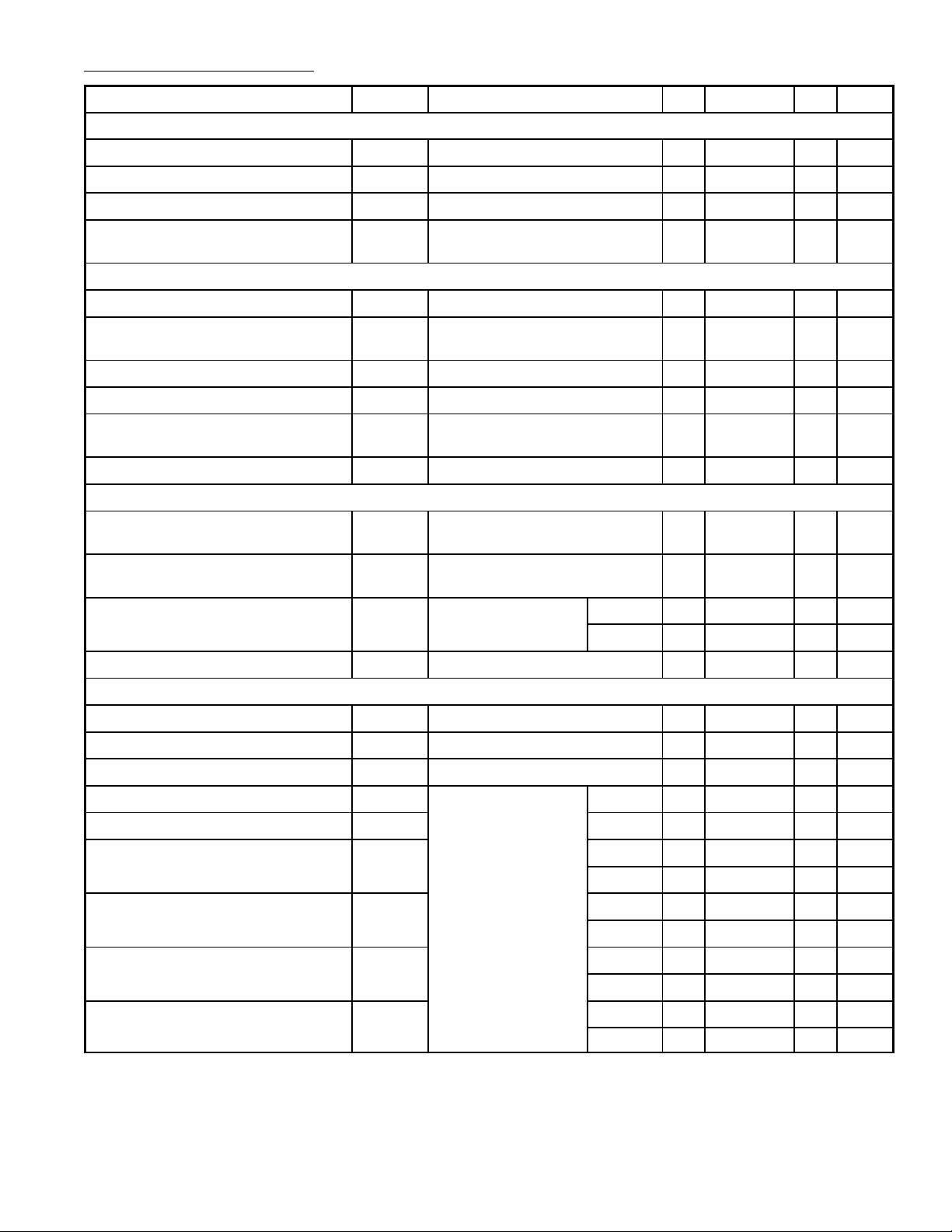
Electrical Characteristics: (TA = +25°C unless otherwise specified)
Parameter Symbol Test Conditions Min Typ Max Unit
Static Characteristics (For Each Differential Amplifier)
Input Offset Voltage V
Input Offset Current I
Input Bias Current I
Temperature Coefficient Magnitude
of Input–Offset Voltage
IO
IO
IB
|∆VIO|
∆T
I3 = I9 = 2mA – 0.3 – µA
(For Each Transistor)
DC Forward Base–Emitter Voltage V
Temperature Coefficient of
∆V
Base–Emitter Voltage
Collector Cutoff Current I
Collector–Emitter Breakdown Voltage V
Collector–Substrate Breakdown Volt-
(BR)CEOIC
V
(BR)CIOIC
BE
∆T
CBO
VCE = 6V, IC = 1mA – 774 – mV
VCE = 6V, IC = 1mA – –0.9 – mV/°
BE
VCB = 10V, IE = 0 – 0.0013 100 nA
= 1mA, IB = 0 15 24 – V
= 10µA, IB = 0, IE = 0 20 60 – V
age
Emitter–Base Breakdown Voltage V
(BR)EBOIE
= 10µA, IC = 0 5 7 – V
Dynamic Characteristics
1/f Noise Figure (For Single Transistor) NF f = 100kHz, RS = 500Ω,
I
= 1mA
C
Gain–Bandwidth Product
f
VCE = 6V, IC = 5mA – 1.38 – GHz
T
(For Single Transistor)
– 0.25 – mV
– 13.5 33 µA
– 1.1 – µV/°C
C
– 1.5 – dB
Collector–Base Capacitance C
CB
IC = 0, VCB = 5V Note 2 – 0.28 – pF
Note 3 – 0.28 – pF
Collector–Substrate Capacitance C
IC = 0, VCI = 5V – 1.65 – pF
CI
(For Each Differential Amplifier)
Common–Mode Rejection Ratio CMR I3 = I9 = 2mA – 100 – dB
AGC Range, One Stage AGC Bias Voltage = –6V – 75 – dB
Voltage Gain, Single–Ended Output A Bias Voltage = –4.2V, f = 10MHz – 22 – dB
Insertion Power Gain G
Noise Figure NF
Input Admittance Y
Reverse Transfer Admittance Y
12
f = 200MHz,
P
VCC = 12V,
For Cascode
11
Configuration
I
= I9 = 2mA
3
For Diff. Amplifier
For Diff. Amplifier
Configuration
Cascode – 23 – dB
Cascode – 4.6 – dB
Cascode – 1.5+j2.45 – mmho
Diff. Amp – 0.878+j1.3 – mmho
Cascode – 0–j0.008 – mmho
Diff. Amp – 0–j0.013 – mmho
I3 = I9 = 4mA
Forward Transfer Admittance Y
Output Admittance Y
21
22
(each Collector
IC ' 2mA
Cascode – 17.9–j30.7 – mmho
Diff. Amp – –10.5+j13 – mmho
Cascode – –0.503–j15 – mmho
Diff. Amp – 0.071+j0.62 – mmho
Note 2. Pins 1 & 12 or Pins 6 & 7.
Note 3. Pins 10 & 11 or Pins 4 & 5.
 Loading...