

NTE NTE903 Datasheet
NTE903
Integrated Circuit
Operational Amplifier
Description:
The NTE903 is an operational amplifier in a 12–Lead TO5 type metal can having all the desirable features and chatacteristics of its prototypes plus a lower noise figure and improved characteristics for
offset voltage, offset current, bias current, and impedance.
Typical Applications:
D Narrow–Band and Band–Pass Amplifier
D Operational Functions
D Feedback Amplifier
D DC and Video Amplifier
D Multivibrator
D Oscillator
D Comparator
D Servo Driver
D Scaling Adder
D Balanced Modulator–Driver
Absolute Maximum Ratings:
(TA = +25°C unless otherwise specified)
Maximum Signal Voltage –8V to +1V. . . . . . . . . . . . . . . . . . . . . . . . . . . . . . . . . . . . . . . . . . . . . . . . . . . . .
Maximum Device Dissipation 600mW. . . . . . . . . . . . . . . . . . . . . . . . . . . . . . . . . . . . . . . . . . . . . . . . . . . .
Operating Temperature Range, T
Storage Temperature Range, T
Lead Temperature (During Soldering, 1/16” from case, 10sec max.), T
Electrical Characteristics:
Parameter Symbol Test Conditions Min Typ Max Unit
Static Characteristics
Input Offset Voltage V
Input Offset Current I
Input Bias Current I
Input Offset Voltage Sensitivity, Positive – 0.096 0.5 mV/V
Input Offset Voltage Sensitivity, Negative – 0.156 0.5 mV/V
Device Dissipation P
opr
stg
L
(TA = +25°C, VCC = ±12V, Note 1 unless otherwise specified)
IO
IO
IB
D
Pin8 shorted to Pin12 – 500 – mW
– 1 2 mV
– 0.5 1.6 µA
– 4.7 6.0 µA
– 175 – mW
–55° to +125°C. . . . . . . . . . . . . . . . . . . . . . . . . . . . . . . . . . . . . . . .
–65° to +200°C. . . . . . . . . . . . . . . . . . . . . . . . . . . . . . . . . . . . . . . . . .
+265°C. . . . . . . . . . . . . . . .
Note 1. Pin5 not connected unless otherwise specified
Electrical Characteristics: (TA = +25°C, VCC = ±12V, Note 1 unless otherwise specified)
Parameter Symbol Test Conditions Min Typ Max Unit
Dynamic Characteristics (All tests at f = 1kHz except BWOL)
Open–Loop Differential Voltage Gain A
Open–Loop Bandwidth BW
OL
–3dB Point 200 320 – kHz
OL
66 70 – dB
Slew Rate SR RS = 1kΩ – 7 – V/µs
Common–Mode Rejection Ratio CMRR 80 103 – dB
Maximum Output–Voltage Swing VO(P–P) 12 14 – V
Input Impedance Z
Output Impedance Z
Common–Mode Input–Voltage Range V
IN
OUT
ICR
7.5 10 – kΩ
– 85 – Ω
+0.65 to –8 V
Noise Figure NF VCC = ±3V, RS = 1kΩ – 6.3 9.0 dB
VCC = ±6V, RS = 1kΩ – 8.3 12 dB
VCC = ±9V, RS = 1kΩ – 10 14 dB
VCC = ±12V, RS = 1kΩ – 11 16 dB
Note 1. Pin5 not connected unless otherwise specified
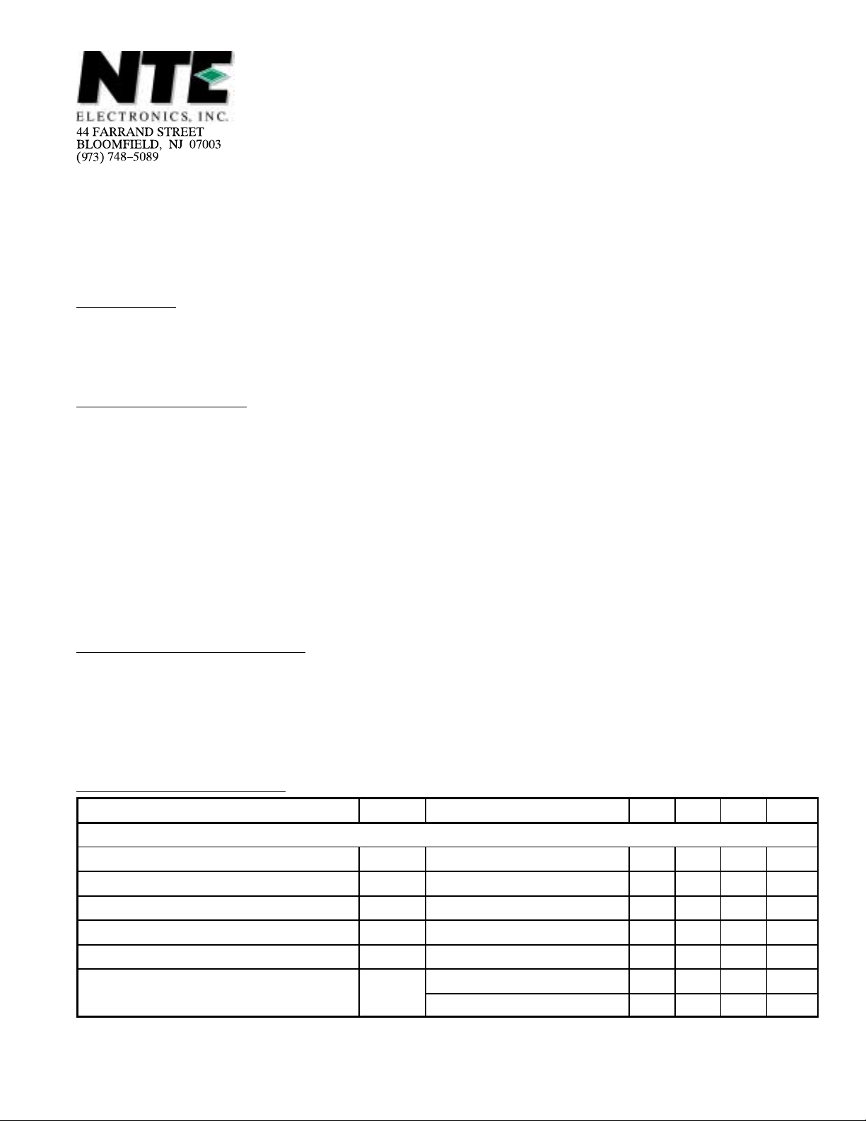
Pin Connection Diagram
(Top View)
Phase Compensation
Output Phase Compensation
8
6
9
7
P–P
V (+) Phase Compensation
Phase Compensation Overload Protection
Phase Compensation
11
12
Bias
10
1
1
2
6
5
4
V (–)
3
Non–Invert Input
Invert Input
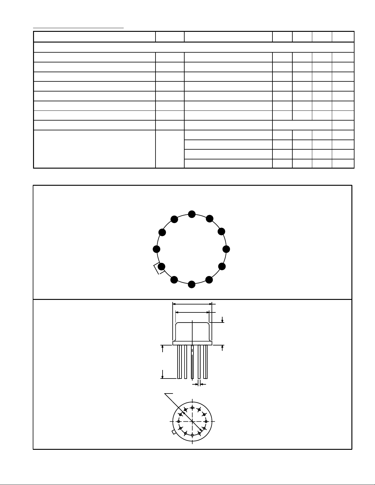
.370 (9.4) Dia Max
.335 (8.5) Dia Max
.180
(4.57)
Max
.500
(12.7)
Min
.018 (0.48) Dia Typ
.245 (6.23) Dia
4
3
2
1
5
6
7
12
8
11
10
9
 Loading...