

NTE NTE894SM, NTE894M Datasheet

NTE894M & NTE894SM
Integrated Circuit
Low Noise Operational Amplifier
Description:
The NTE891M and NTE891SM are single, high–performance, low noise operational amplifiers.
Compared to other operational amplifier, these devices show better noise performance, improved
output drive capability and considerably higher small–signal and power bandwidths.
This makes the devices especially suitable for applications in high quality and professional audio
equipment, in instrumentation and control circuits and telephone channel amplifiers. The OP amps
are internally compensated for gain equal to, or higher than, three.
Features:
D Small–Signal Bandwidth
D Large Supply Voltage Range
D Available in 8–Lead Mini DIP (NTE894M) and Surface Mount SOIC–8 (NTE894SM)
Applications:
D Audio Equipment
D Instrumentation and Control Circuits
D Telephone Channel Amplifiers
D Medical Equipment
Absolute Maximum Ratings:
Supply Voltage, V
Differential Input Voltage (Note 1), V
Input Voltage, V
S
DIFF
IN
Power Dissipation (TA = +25°C, Note 2), P
±V supply V. . . . . . . . . . . . . . . . . . . . . . . . . . . . . . . . . . . . . . . . . . . . . . . . . . . . . . . . . . .
D
±22V. . . . . . . . . . . . . . . . . . . . . . . . . . . . . . . . . . . . . . . . . . . . . . . . . . . . . . . . . . . . . . . .
±0.5V. . . . . . . . . . . . . . . . . . . . . . . . . . . . . . . . . . . . . . . . . . . .
1150mW. . . . . . . . . . . . . . . . . . . . . . . . . . . . . . . . . . . . . . .
Output Short–Circuit Duration (Note 3) Indifinite. . . . . . . . . . . . . . . . . . . . . . . . . . . . . . . . . . . . . . . . . . . .
Operating Temperature Range, T
Storage Temperature Range, T
opr
stg
Lead Soldering Temperature (10 seconds), T
L
0° to +70°C. . . . . . . . . . . . . . . . . . . . . . . . . . . . . . . . . . . . . . . . . . .
–65° to +150°C. . . . . . . . . . . . . . . . . . . . . . . . . . . . . . . . . . . . . . . . . .
+300°C. . . . . . . . . . . . . . . . . . . . . . . . . . . . . . . . . . . . . .
Note 1. Diodes protect the inputs against over voltage. Therefore, unless current limiting resistors
are used, large currents will flow if the differential input voltage exceeds 0.6V. maximum current should be limited to ±10mA.
Note 2. For operation at elevated temperature, derate packages based on the following junction–to–
ambient thermal resistance: NTE894M 105°C/W; NTE894SM 160°C/W.
Note 3. Output may be shorted to GND at VS = 15V , TA = +25°C. Temperature and/or supply voltages
must be limited to ensure dissipation rating is not exceeded.
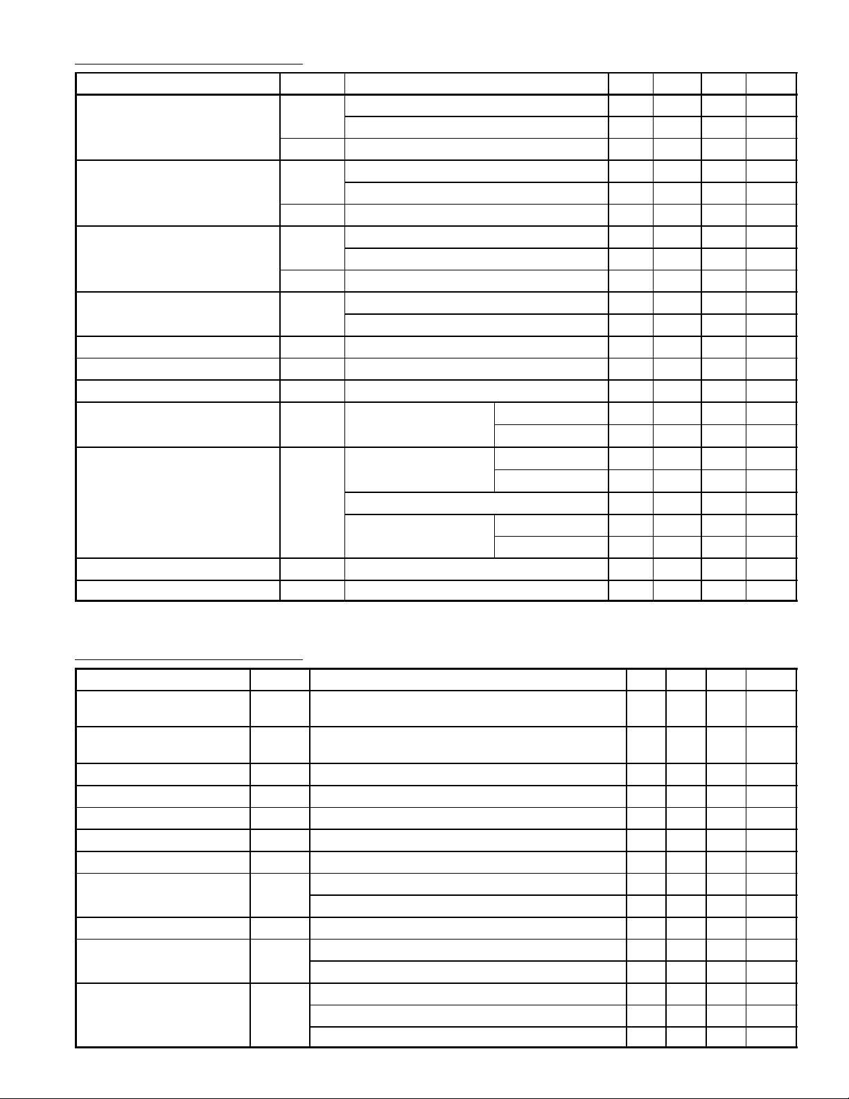
DC Electrical Characteristics: (TA = +25°C, VS = ±15V, unless otherwise specified)
Parameter Symbol Test Conditions Min Typ Max Unit
Input Offset Voltage V
OS
TA = 0° to +70°C – – 5 mV
∆VOS/∆T – 5 – µV/°C
Input Offset Current I
OS
TA = 0° to +70°C – – 400 nA
∆IOS/∆T – 200 – pA/°C
Input Bias Current I
B
TA = 0° to +70°C – – 2000 nA
∆IB/∆T – 5 – nA/°C
Supply Current I
CC
TA = 0° to +70°C – – 10 mA
Input Common–Mode Range V
CM
Common–Mode Rejection Ratio CMRR 70 100 – dB
Power Supply Rejection Ratio PSRR – 10 100 µV/V
Large–Signal Voltage Gain A
VOL
RL ≥ 600Ω, VO = ±10V
TA = 0° to +70°C 15 – – V/mV
Output Voltage Swing V
OUT
RL ≥ 600Ω ±12 ±13 – V
TA = 0° to +70°C ±10 ±12 – V
RL ≥ 600Ω, VO = ±18V ±15 ±16 – V
RL ≥ 2kΩ ±13 ±13.5 – V
TA = 0° to +70°C ±12 ±12.5 – V
Input Resistance R
Output Short–Circuit Current I
IN
SC
– 0.5 4 mV
– 20 300 nA
– 500 1500 nA
– 4 8 mA
±12 ±13 – V
25 100 – V/mV
50 100 – kΩ
– 38 – mA
AC Electrical Characteristics: (TA = +25°C, VS = ±15V unless otherwise specified)
Parameter Symbol Test Conditions Min Typ Max Unit
Output Resistance R
Transient Response Voltage Follower, VIN = 50mV, RL = 600Ω,
Rise Time t
Overshoot – 20 – %
Transient Response VIN = 50mV, RL = 600Ω, CC = 47pF, CL = 500pF
Rise Time t
Overshoot – 35 – %
Gain A
Gain Bandwidth Product GBW CC = 22pF, CL = 100pF – 10 – MHz
Slew Rate SR CC = 0 – 13 – V/µs
Power Bandwidth V
OUT
R
R
V
AV = 30dB, Closed–Loop, f = 10kHz, RL = 600Ω,
– 0.3 – Ω
CC = 22pF
CC = 22pF, CL = 100pF
– 20 – ns
– 50 – ns
f = 10kHz, CC = 0 – 6 – V/mV
f = 10kHz, CC = 22pF – 2.2 – V/mV
CC = 22pF – 6 – V/µs
= ±10V, CC = 0 – 200 – kHz
OUT
V
= ±10V, CC = 22pF – 95 – kHz
OUT
V
= ±14V, RL = 600Ω, CC = 22pF, VCC = ±18V – 70 – kHz
OUT
 Loading...