

NTE NTE891M, NTE891SM Datasheet

NTE891M & NTE891SM
Integrated Circuit
Dual Audio Operational Amplifier
Description:
The NTE891M and NTE891SM are dual general purpose operational amplifiers designed with particular emphasis on performance in audio systems. Thiese devices deliver low noise, high speed and
wide bandwidth without increasing external components for all closed loop gains and is therefore optimized for all preamp and high level stages in PCM and HiFi systems.
Features:
D Wide Dynamic Range
D Low Input Noise Voltage
D High Slew Rate
D High Gain Bandwidth Product
D Wide Power Bandwidth
D Low Distortion
D Low Offset Voltage
D Large Phase Margin
D Available in 8–Lead Mini DIP (NTE891M) and Surface Mount SOIC–8 (NTE891SM)
Absolute Maximum Ratings:
Supply Voltage, V
Differential Input Voltage (Note 1), V
Input Voltage Range (Note 1), V
Power Dissipation (Note 2), P
Operating Temperature Range, T
Storage Temperature Range, T
Lead Soldering Temperature (10 seconds), T
CC
– V
EE
ID
IC
D
opr
stg
L
Note 1. If supply voltage is less than ±15V, it is equal to supply voltage.
Note 2. This is a permissible value at T
≤ +85°C.
A
36V. . . . . . . . . . . . . . . . . . . . . . . . . . . . . . . . . . . . . . . . . . . . . . . . . . . . . . . . . .
±30V. . . . . . . . . . . . . . . . . . . . . . . . . . . . . . . . . . . . . . . . . . . . . . .
±15V. . . . . . . . . . . . . . . . . . . . . . . . . . . . . . . . . . . . . . . . . . . . . . . . . . .
500mW. . . . . . . . . . . . . . . . . . . . . . . . . . . . . . . . . . . . . . . . . . . . . . . . . . .
–40° to +85°C. . . . . . . . . . . . . . . . . . . . . . . . . . . . . . . . . . . . . . . . .
–60° to +150°C. . . . . . . . . . . . . . . . . . . . . . . . . . . . . . . . . . . . . . . . . .
+260°C. . . . . . . . . . . . . . . . . . . . . . . . . . . . . . . . . . . . . .
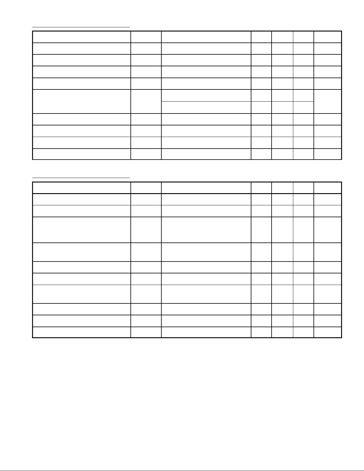
DC Electrical Characteristics: (TA = +25°C, VS = ±15V, unless otherwise specified)
Parameter Symbol Test Conditions Min Typ Max Unit
Input Offset Voltage V
Input Offset Current I
Input Bias Current I
Voltage Gain A
Output Voltage Swing V
OS
OS
B
OM
RS = 10Ω – 0.3 5 mV
– 10 200 nA
– 500 1000 nA
RL = 2kΩ, VO = ±10V 90 110 – dB
V
RL = 10kΩ ±12 ±13.5 –
V
RL = 2kΩ ±10 ±13.4 –
Input Common–Mode Range V
CM
±12 ±14.0 – V
Common–Mode Rejection Ratio CMRR VIN = ±12V 80 100 – dB
Power Supply Rejection Ratio PSRR VS = 15V to 5V, –15V to –5V 80 100 – dB
Supply Current I
Q
VO = 0V, Both Amps – 5 8 mA
AC Electrical Characteristics: (TA = +25°C, VS = ±15V, RL = 2kΩ, unless otherwise specified)
Parameter Symbol Test Conditions Min Typ Max Unit
Slew Rate SR RL = 2kΩ 5 7 – V/µs
Gain Bandwidth Product GBW f = 100kHz 10 15 – MHz
Average Temperature
∆VOS/∆T – 2 – µV/°C
Coefficient of Input Offset
Voltage
Distortion THD RL = 2kΩ, f = 20 ∼ 20kHz,
Input Referred Noise Voltage e
Input Referred Noise Current i
= 3V
V
OUT
RS = 100Ω, f = 1kHz – 4.5 – nV/√Hz
n
n
f = 1kHz – 0.7 – pA/√Hz
, AV = 1
rms
Power Bandwidth PBW VO = 27Vpp, RL = 2kΩ,
– 0.002 – %
– 120 – kHz
THD ≤ 1%
Unity Gain Frequency f
Phase Margin φ
U
M
Open Loop – 9 – MHz
Open Loop – 60 – deg
Input Referred Cross Talk f = 20 ∼ 20kHz – –120 – dB
 Loading...