

NTE NTE890 Datasheet

NTE890
Integrated Circuit
Voltage to Frequency Converter
Description:
The NTE890 is an integrated circuit in an 8–Lead DIP type package and provides a simple method
of A/D conversion. It has all the inherent advantages of the voltage–to–frequency conversion technique. The output is a series of constant duration pulses. The frequency of the pulses is proportional
to the applied input voltage. This converter is designed for use in a wide range of data conversion
and remote sensing applications.
Absolute Maximum Ratings
: (TA = +25°C unless otherwise specified)
Supply Voltage, V+ 8V to 22V. . . . . . . . . . . . . . . . . . . . . . . . . . . . . . . . . . . . . . . . . . . . . . . . . . . . . . . . . . . .
Output Sink Current, I
Power Dissipation, P
Input Voltage, V
i
Operating Temperature Range, T
Storage Temperature Range, T
Electrical Characteristics
Parameter Test Conditions Min Typ Max Unit
Supply Current 8V < V+ < 15V 2.0 3.5 6.0 mA
Conversion Accuracy Scale Factor VIN = 10V, RS = 14kΩ 0.9 1.0 1.1 kHz/V
Drift with Temperature VIN = 10V – ±100 – ppM/°C
Drift with V+ VIN = 1V, 8V < V+ < 18V – 0.2 1.0 %/V
Input Comparator Offset Voltage – 5 10 mV
Offset Current – ±50 ±100 nA
Input Bias Current – –100 –300 nA
SINK
D
opr
stg
: (V+ = +15V, TA = +25°C unless otherwise specified)
15V < V+ < 22V 2.0 4.5 7.5 mA
–0.2V to V+(V). . . . . . . . . . . . . . . . . . . . . . . . . . . . . . . . . . . . . . . . . . . . . . . . . . . . . . . . . .
–20° to +75°C. . . . . . . . . . . . . . . . . . . . . . . . . . . . . . . . . . . . . . . . .
–40° to +125°C. . . . . . . . . . . . . . . . . . . . . . . . . . . . . . . . . . . . . . . . . .
20mA. . . . . . . . . . . . . . . . . . . . . . . . . . . . . . . . . . . . . . . . . . . . . . . . . . . . . . . . .
500mW. . . . . . . . . . . . . . . . . . . . . . . . . . . . . . . . . . . . . . . . . . . . . . . . . . . . . . . . . .
Common Mode Range Note 1 0 to V+ –3 0 to V+ –2 – V
One–Shot Threshold Voltage Pin5 0.63 0.66 0.70 x V+
Input Bias Current Pin5 – –100 –500 nA
Reset V
SAT
Pin5, I = 2.2mA – 0.15 0.50 V
Note 1 Input Common Mode Range includes GND.
Electrical Characteristics (Cont’d): (V+ = +15V, TA = +25°C unless otherwise specified)
Parameter Test Conditions Min Typ Max Unit
Current Source
Output Current
Change with Voltage Pin1, V+ = 0V to 10V – 1.0 2.5 µA
Off Leakage Pin1, V+ = 0V – 1 50 nA
Reference Voltage Pin2 1.70 1.90 2.08 V
RS = 14kΩ, Pin1, V+ = 0V – 138.7 – µA
Logic Output V
V
SAT
Off Leakage – 0.1 1.0 µA
SAT
Pin3, I = 3mA – 0.15 0.50 V
Pin3, I = 2mA – 0.10 0.30 V
Note 2. The voltage applied to comparator input Pin6 and Pin7 should not be allowed to go below
GND by more than 300mV.
Note 3. Pin3 and Pin5 are open–collector outputs. Shorts between these pins and V+ can cause
overheating and eventual destruction.
Note 4. Reference voltage terminal Pin2 is connected to the emitter of an NPN transistor and is held
at approximately 1.9V. This terminal should be protected from accidental shorts to GND or
supply voltages. Permanent damage may occur if current in Pin2 exceeds 5mA.
Note 5. Avoid stray coupling between Pin5 and Pin7 which could cause false triggering. If false trig-
gering is experienced with the precision mode circuits, bypass Pin6 to GND with at least
0.01µF. This is necessary for operation above 10kHz.
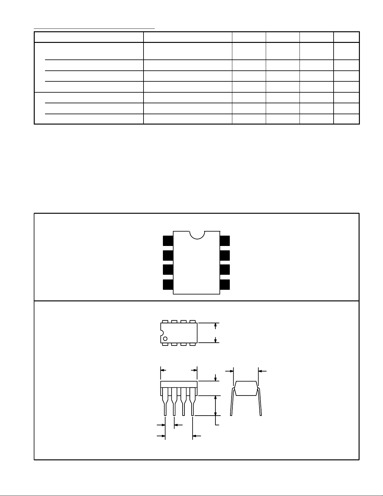
Pin Connection Diagram
Current Source
Scale Factor12
Logic Output
3
V
8
CC
Input Voltage
7
6
Threshold
GND
.100 (2.54)
4
85
.260 (6.6)
14
.390 (9.9)
Max
.155
(3.93)
.300 (7.62)
5
One–Shot R, C
.300
(7.62)
.145 (3.68)
 Loading...