

NTE NTE887M Datasheet

NTE887M
Integrated Circuit
Low Power, JFET OP Amplifier
Description:
The NTE887M is a JFET–input operational amplifier in an 8–Lead DIP type package designed as a
low–power version of the NTE857M amplifier . This device features high input impedance, wide bandwidth, high slew rate, and low input offset and bias current.
Features:
D Very Low Power Consumption
D Typical Supply Current: 200µA
D Wide Common–Mode and Differential Voltage Ranges
D Low Input Bias and Offset Currents
D Common–Mode Input Voltage Range Includes V
D Output Short–Circuit Protection
D High Input Impedance: JFET–Input Stage
D Internal Frequency Compensation
D Latch–Up–Free Operation
D High Slew rate: 3.5V/µs Typ
CC
+
Absolute Maximum Ratings:
Supply Voltage (Note 1), V
Supply Voltage (Note 1), V
Differential Input Voltage (Note 2), V
Input Voltage (Note 1, Note 3), V
Duration of Output Short Circuit (Note 4), t
Continuous Total Dissipation, P
(TA = 0° to +70°C unless otherwise specified)
+ +18V. . . . . . . . . . . . . . . . . . . . . . . . . . . . . . . . . . . . . . . . . . . . . . . . . . . . . .
CC
– –18V. . . . . . . . . . . . . . . . . . . . . . . . . . . . . . . . . . . . . . . . . . . . . . . . . . . . . .
CC
ID
I
s
D
±30V. . . . . . . . . . . . . . . . . . . . . . . . . . . . . . . . . . . . . . . . . . . . . . .
±15V. . . . . . . . . . . . . . . . . . . . . . . . . . . . . . . . . . . . . . . . . . . . . . . . . . . .
Unlimited. . . . . . . . . . . . . . . . . . . . . . . . . . . . . . . . . . . . . . .
TA ≤ +25°C 680mW. . . . . . . . . . . . . . . . . . . . . . . . . . . . . . . . . . . . . . . . . . . . . . . . . . . . . . . . . . . . . .
Derate Above +65°C 8mW/°C. . . . . . . . . . . . . . . . . . . . . . . . . . . . . . . . . . . . . . . . . . . . . . . . . . .
T
= +70°C 640mW. . . . . . . . . . . . . . . . . . . . . . . . . . . . . . . . . . . . . . . . . . . . . . . . . . . . . . . . . . . . . .
A
Operating Ambient Temperature Range, T
Storage Temperature range, T
stg
A
Lead Temperature (During Soldering, 1/16” (1.6mm) from case for 10sec), T
L
0° to +70°C. . . . . . . . . . . . . . . . . . . . . . . . . . . . . . . . . . . . .
–65° to +150°C. . . . . . . . . . . . . . . . . . . . . . . . . . . . . . . . . . . . . . . . . . .
+260°C. . . . . . . . . . .
Note 1. All voltage values, except differential voltages, are with respect to the midpoint between
V
+ and VCC–.
CC
Note 2. Differential voltages are at the non–inverting input pin with respect to the inverting input pin.
Note 3. The magnitude of the input voltage must never exceed the magnitude of the supply voltage
or 15V, whchever is less.
Note 4. The output may be shorted to GND or to either supply. Temperature and/or supply voltages
must be limited to ensure that the dissipation rating is not exceeded.
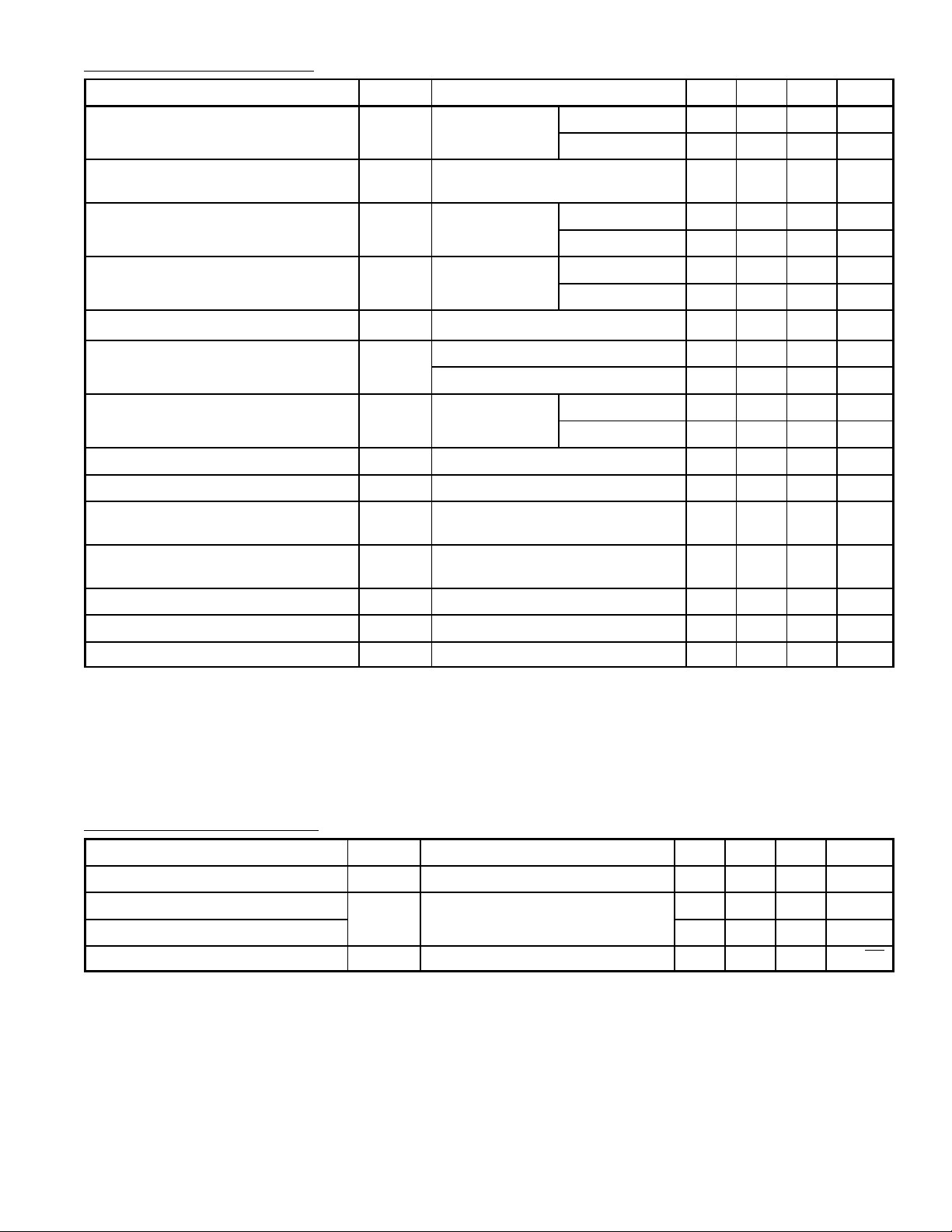
Electrical Characteristics: (VCC± = ±15V, Note 5 unless otherwise specified)
Parameter Symbol Test Conditions Min Typ Max Unit
Input Offset Voltage V
Temperature Coefficient of
a
IO
VIO
VO = 0,
RS = 50Ω
VO = 0, RS = 50Ω, TA = 0° to +70°C – 10 – µV/°C
TA = +25°C – 3 15 mV
TA = 0° to +70°C – – 20 mV
Input Offset Voltage
Input Offset Current I
IO
VO = 0, Note 6 TA = +25°C – 5 200 pA
TA = 0° to +70°C – – 5 nA
Input Bias Current I
IB
VO = 0, Note 6 TA = +25°C – 30 400 pA
TA = 0° to +70°C – – 10 nA
Common–Mode Input Voltage Range V
Maximim Peak Output Voltage Swing V
ICR
OM
TA = +25°C ±11
RL = 10kΩ, TA = +25°C ±10.0 ±13.5 – V
–12
+15
– V
RL ≥ 10kΩ, TA = 0° to +70°C ±10.0 – – V
Large–Signal Differential Voltage
A
VD
VO = ±10V,
Amplification RL ≥ 10kΩ
Unity–Gain Bandwidth B
Input Resistance r
RL = 10kΩ, TA = +25°C – 1 – MHz
1
TA = +25°C – 10
i
Common–Mode Rejection Ratio CMRR VIC = V
= +25°C
T
A
Supply Volatge Rejection Ratio
±/∆VIO)
(∆V
CC
Total Power Dissipation P
Supply Current I
k
SVR
D
CC
VCC = ±15V to ±9V, VO = 0,
= 50Ω, TA = +25°C
R
S
No Load, VO = 0, TA = +25°C – 6.0 7.5 mW
No Load, VO = 0, TA = +25°C – 200 250 µA
min, VO = 0, RS = 50Ω,
ICR
TA = +25°C 3 6 – V/mV
TA = 0° to +70°C 3 – – V/mV
12
– Ω
70 86 – dB
70 95 – dB
Crosstalk Attenuation Vo1/Vo2AVD = 100, TA = +25°C – 120 – dB
Note 5. All characteristics are measured under open–loop conditions with zero common–mode volt-
age unless otherwise specified.
Note 6. Input bias currents of a FET–input operational amplifier are normal junction reverse currents,
which are temperature sensitive. Pulse techniques must be used that will maintain the junction temperature as close to the ambient temperature as possible.
Operating Characteristics:
Parameter Symbol Test Conditions Min Typ Max Unit
Slew Rate at Unity Gain SR VI = 10V, RL = 10kΩ, CL = 100pF 1.5 3.5 – V/µs
Rise Time t
Overshoot Factor
Equivalent Input Noise Voltage V
(VCC± = ±15V, TA = +25°C unless otherwise specified)
VI = 20mV, RL = 10kΩ, CL = 100pF – 0.2 – µs
r
– 10% –
RS = 100Ω, f = 1kHz – 42 – nV/√Hz
n
 Loading...