

NTE NTE874 Datasheet

NTE874
Integrated Circuit
TV Horiz/Vert Countdown System Circuit
Description:
The NTE874 is a monolithic bipolar/I2L integrated circuit digital sync system designed for use in consumer TV applications for color/monochrome receivers or monitors. This device takes the composite
video input signal in combination with the on–chip master–scan oscillator to provide both horizontal
drive and vertical deflection output signals.
Other on–chip functions include sync separator, horizontal APC, horizontal/vertical count–down circuitry, vertical ramp generator, and horizontal drive circuit (Pulse–Width Modulator).
The NTE874 features dual–mode operation and accepts either standard or non–standard video signals. An automatic mode–recognition system forces the operation into the asynchronous mode for
non–standard sync signals.
Intended for use with 525–line systems, the NTE874 is supplied in the 28–lead dual–in–line plastic
package.
Features:
D Sync Separator
D Master Scan Oscillator (at 64 X f
D Automatic Phase Control (APC) of Oscillator
D Horizontal/Vertical Count–down
D Vertical Output
D Horizontal Drive Output (Pulse–Width Modulator)
)
H
Absolute Maximum Ratings
POWER SUPPLY:
Power Supply Voltage, V
Power Supply Current, I
Injector Supply Voltage, V
Injector Supply Current, I
15V. . . . . . . . . . . . . . . . . . . . . . . . . . . . . . . . . . . . . . . . . . . . . . . . . . . . . . . . .
CC
75mA. . . . . . . . . . . . . . . . . . . . . . . . . . . . . . . . . . . . . . . . . . . . . . . . . . . . . . . .
CC
INJ
150mA. . . . . . . . . . . . . . . . . . . . . . . . . . . . . . . . . . . . . . . . . . . . . . . . . . . . . .
INJ
:
1.75V. . . . . . . . . . . . . . . . . . . . . . . . . . . . . . . . . . . . . . . . . . . . . . . . . . . . . .
Absolute Maximum Ratings (Cont’d):
INPUTS OUTPUTS:
AGC Gate (Pin 9) Source, I
Composite Blanking (Pin 16) Sink, I
Horizontal Drive (Pin 5) Sink, I
Horizontal Output (Pin 3) Sink, I
Sync Separator Out (Pin 28), I
Vertical Drive (Pin 14) Source, I
EAGC
CHD
SYNC
CBLNK
10mA. . . . . . . . . . . . . . . . . . . . . . . . . . . . . . . . . . . . . . . . . . .
50mA. . . . . . . . . . . . . . . . . . . . . . . . . . . . . . . . . . . . . . . . . . . . . . . . .
30mA. . . . . . . . . . . . . . . . . . . . . . . . . . . . . . . . . . . . . . . . . . . . . . . .
CHO
30mA. . . . . . . . . . . . . . . . . . . . . . . . . . . . . . . . . . . . . . . . . . . . . . . .
50mA. . . . . . . . . . . . . . . . . . . . . . . . . . . . . . . . . . . . . . . . . . . . . . .
VERT
DEVICE DISSIPATION:
Maximum Rated Junction Temperature, T
Maximim Power Dissipation, P
D
+150°C. . . . . . . . . . . . . . . . . . . . . . . . . . . . . . . . . . . . .
JMAX
Up to TA = +50°C 1.1W. . . . . . . . . . . . . . . . . . . . . . . . . . . . . . . . . . . . . . . . . . . . . . . . . . . . . . . . . . .
Above T
= +50°C Derate linearly at 11.1 mW/°C. . . . . . . . . . . . . . . . . . . . . . . . . . . . . . . . . . . .
A
AMBIENT TEMPERATURE RANGE:
Operating, T
Storage, T
0° to +85°C. . . . . . . . . . . . . . . . . . . . . . . . . . . . . . . . . . . . . . . . . . . . . . . . . . . . . . . . . . . . .
OP
–55° to +150°C. . . . . . . . . . . . . . . . . . . . . . . . . . . . . . . . . . . . . . . . . . . . . . . . . . . . . . . . . . .
STG
LEAD TEMPERATURE (DURING SOLDERING):
At distance 1/16 ± 1/32 in. (1.59 ± 0.79mm) from case for 10s max. +265°C. . . . . . . . . . . . . . . . . . . .
10mA. . . . . . . . . . . . . . . . . . . . . . . . . . . . . . . . . . . . . . . . . . . . . . . . . . .
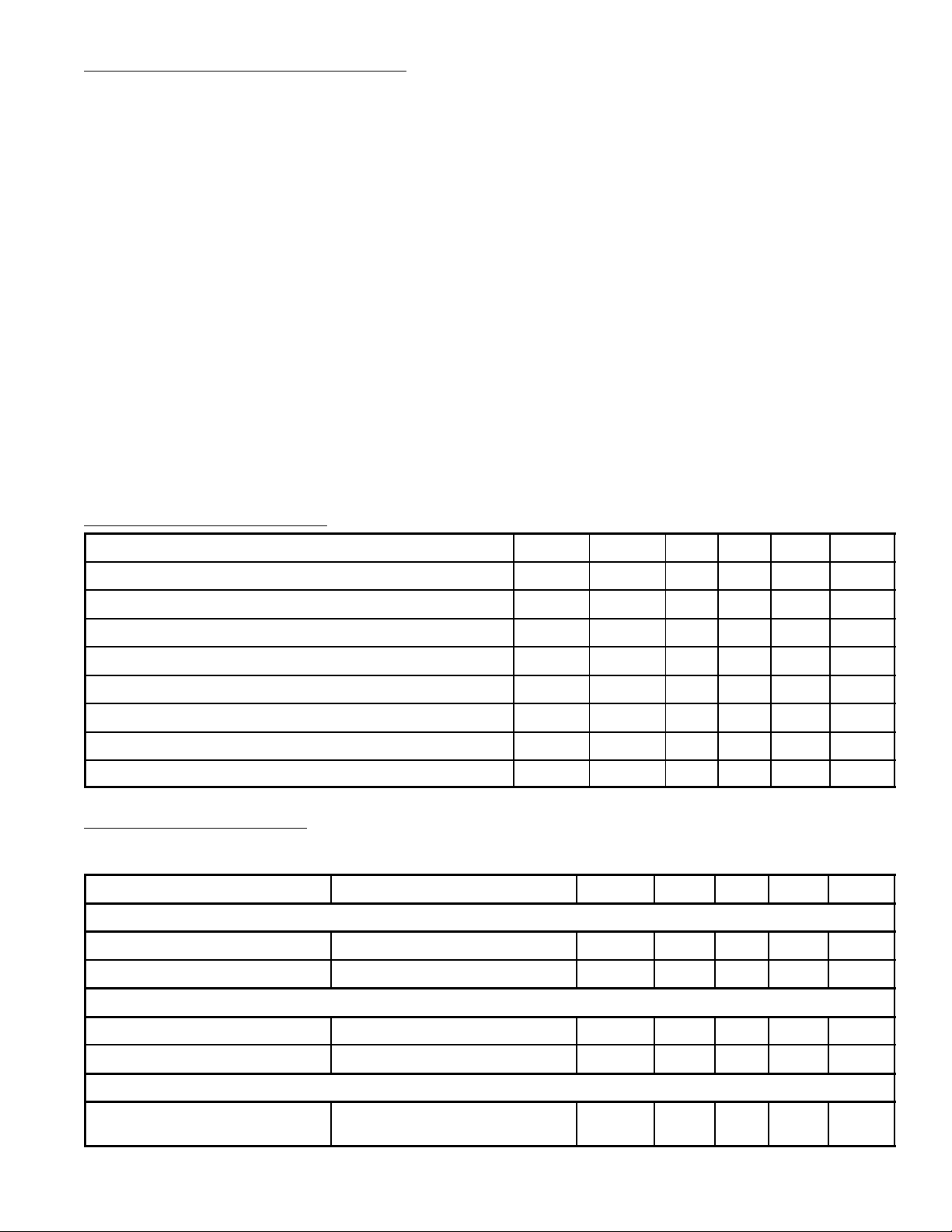
Standard Operating Range:
Parameter Symbol PIN # Min Typ Max Units
Analog Supply Voltage V
Analog Supply Current I
Injector Supply Voltage V
Total Dissipation, no external loads P
Force Asynchronous Low (“0”) V
Force Asynchronous V
Integrated Vertical, Low V
Integrated Vertical, High V
CC
CC
INJ
D
FAL
FAH
IVL
IVH
7 10.9 12.0 12.9 V
7 30 45 60 mA
10 1.3 1.6 1.9 V
– – 580 – mW
2 –0.5 0 +0.25 V
2 0.7 0.8 1.5 V
1 – – 1.9 V
1 2.8 – – V
Electrical Characteristics: (TA = +25°C, VCC = 12VDC, V25 = 12VDC, Pin 2, 15, 22 to GND;, 1µF
from Pin 4 to GND., 10K ohms from Pin 28 to GND., F
4V, V
Power Supply Section
Supply Current Pin 10 Open 7 20 45 60 mA
1.9V to 2.8V, VFA 0.2V to 0.7V)
IV
Parameter Test Conditions PIN # Min Typ Max Units
= 1MHz, (AC Coupled), V
CLK
Sync
1.2V to
Injector Voltage 10 1.3 1.6 1.9 V
Sync Separator/Diff. Section
Video Inverter, High Voltage V27 = 4V, I26 = –500µA 26 4.2 5.1 5.8 V
Sync Processor, Low Voltage V27 = 4V, I26 = 0µA 28 – – .1 V
OSC/Count–Down/APC Section
APC Bias V27 = 4V, I26 = 0µA,
21 6.5 6.8 7.5 V
V21 = Open
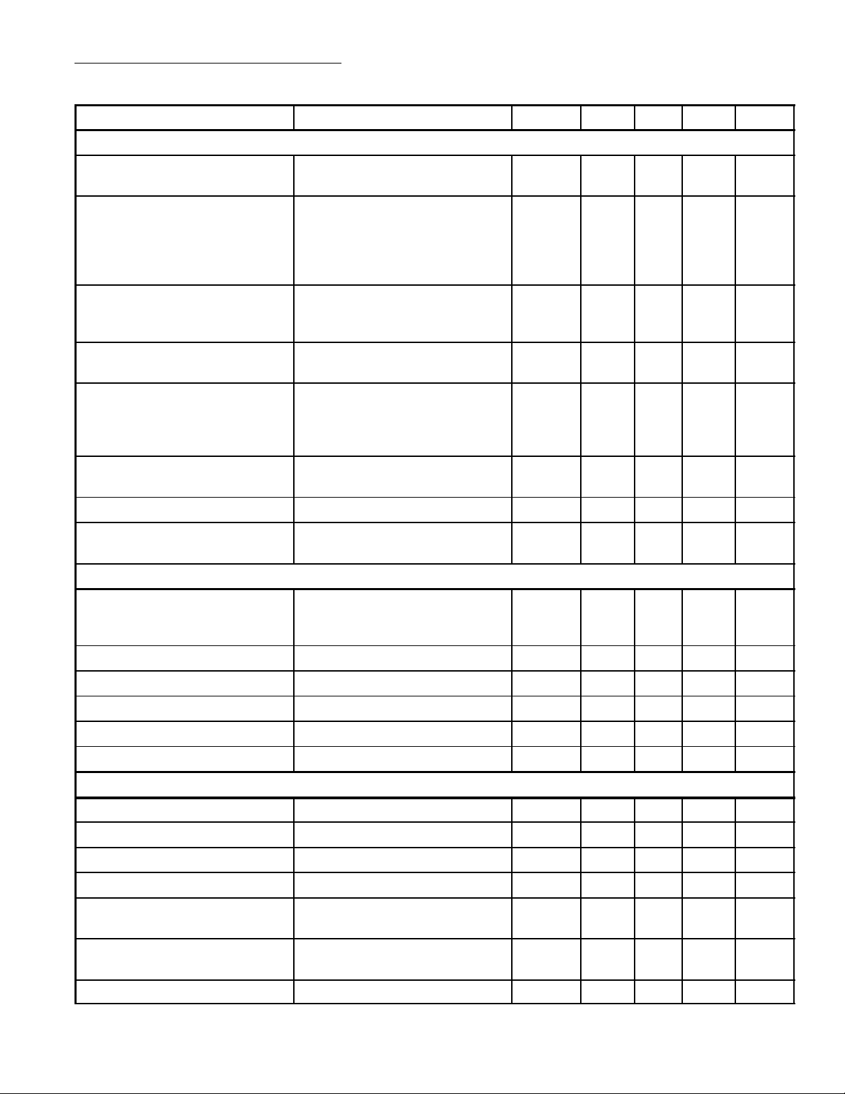
Electrical Characteristics (Cont’d): (TA = +25°C, VCC = 12VDC, V25 = 12VDC, Pin 2, 15, 22 to
GND;, 1µF from Pin 4 to GND., 10K ohms from Pin 28 to GND., F
1.2V to 4V, VIV 1.9V to 2.8V, VFA 0.2V to 0.7V)
V
Sync
Parameter Test Conditions PIN # Min Typ Max Units
OSC/Count–Down/APC Section (Cont’d)
= 1MHz, (AC Coupled),
CLK
APC Discharge V27 = 4V, I26 = 0µA,
21 6.5 6.8 7.5 V
V21 = Open
APC Discharge I26 = –500µA, V20 = 2V,
21 600 803 1100 µA
V21 = 2V,
V21 = VAPC Bias (above),
(Stop Clock When Pin 21
Goes Low)
APC Charge V27 = 4V, I26 = –500µA,
21 –600 –793 –1100 µA
V20 = 6V,
V21 = VAPC Bias (above)
Phase Detector I21 = APC Discharge–APC
21 –30 9.8 30 µA
Charge
Sync Width, Wide
Differentiation
V27 = 5V, V23 = 1MHz,
I20 = –300µA,
21 5 6 8 µs
V26 = Sq. Wave 0 to 5V with
T
= T
on
Sync Width, Narrow Same as above except
T
on
= 31.75µs
off
= 2µs, T
= 61.5µs
off
21 1.8 2.3 2.6 µs
Phase Detector Bias V27 = 4V 20 3.9 4.3 4.7 V
Oscillator Current 1 V24 = 3V, V23 = 6V
25 1.4 1.8 3.0 mA
V21 = 8.5V
OSC/Count–Down/APC Section
Oscillator Current Ratio V24 = 3V, V23 = 6V,
25 .45 .5 .55 Ratio
V21 = Open, Measured I25 &
Divide by Oscillator Current 1
Oscillator Bias 24 4.5 4.8 5.5 V
+Phase Input Current V24 = 0V 24 –230 312 –570 µA
–Phase Input Current V23 = 0V 23 –230 331 –570 µA
Flyback Charge Current V17 = 0V, V19 = 6V 19 –400 –501 –766 µA
Flyback Discharge Current I17 = 700µA, V19 = 6V 19 2 2.4 3.5 mA
Blanking/Gating Section
Flyback Input, Low Current 1 V18 = 0V 18 –3 –1 3 µA
Flyback Input, High Current 1 V18 = 2V 18 0.8 1.6 3.8 mA
Flyback Input, Low Current 2 V17 = 0V 17 –3 –.09 3 µA
Flyback Input, High Current 2 V17 = 2V 17 0.8 1.5 1.9 mA
Blanking Voltage V18 = 2V, V23 = 1MHz, Stop
16 5.8 6 6.4 V
Clock when 3V < V16< 5V
Burst Voltage V18 = 2V, V23 = 1MHz, Stop
16 11.2 11.95 – V
Clock when V16 > 9V
Burst Saturation Voltage V18 = 0V I16 = 5µA 16 – .45 0.6 V
 Loading...