

NTE NTE863 Datasheet

NTE863
Integrated Circuit
OP Amp/Comparator
Description:
The NTE863 is a multiple–control amplifier/comparator monolithic integrated circuit in an 8–Lead DIP
type package intended for use in general purpose applications requiring comparator functions wiht
logic override switching and control. An op–amp with differential inputs drives an output transistor
with high current capability. An isolated transistor is also available for optional use.
Features:
D High Output Current (50 mA max)
D Output Sink Current or Drive Current Capability
D Output Disable Control
Applications:
D Comparator
D Switching and Gating Control
D Pulse Width Modulator
D TV Horizontal Drive Amplifier
Absolute Maximum Ratings:
DC Supply Voltage, V1, V
Input Current, I
Output Current, I
Output Current, I
, I4, I7, I
3
1
6
Device Dissipation (T
5
8
≤ +25°C, Including Q14), P
A
D
Derate Linearly Above 25°C 5mW/°C. . . . . . . . . . . . . . . . . . . . . . . . . . . . . . . . . . . . . . . . . . . . . . .
Q14 Dissipation (T
≤ +25°C), P
A
D
Derate Linearly Above 25°C 1.2mW/°C. . . . . . . . . . . . . . . . . . . . . . . . . . . . . . . . . . . . . . . . . . . . .
Operating Ambient Temperature Range, T
Storage Temperature Range, T
stg
opr
Lead Temperature (During Soldering, 1/16” from case, 10sec max), T
+15V. . . . . . . . . . . . . . . . . . . . . . . . . . . . . . . . . . . . . . . . . . . . . . . . . . . . . . . . . .
±1mA. . . . . . . . . . . . . . . . . . . . . . . . . . . . . . . . . . . . . . . . . . . . . . . . . . . . . . . . . .
50mA. . . . . . . . . . . . . . . . . . . . . . . . . . . . . . . . . . . . . . . . . . . . . . . . . . . . . . . . . . . . . . . .
10mA. . . . . . . . . . . . . . . . . . . . . . . . . . . . . . . . . . . . . . . . . . . . . . . . . . . . . . . . . . . . . . . .
625mW. . . . . . . . . . . . . . . . . . . . . . . . . . . . . . . . .
150mW. . . . . . . . . . . . . . . . . . . . . . . . . . . . . . . . . . . . . . . . . . . . . . . .
0° to +70°C. . . . . . . . . . . . . . . . . . . . . . . . . . . . . . . . . . . .
–65° To +150°C. . . . . . . . . . . . . . . . . . . . . . . . . . . . . . . . . . . . . . . . .
L
+265°C. . . . . . . . . . . . . . . . .
Electrical Characteristics: (TA = +25°C, V+ (V5) = 15V unless otherwise specified)
Parameter Symbol Test Conditions Min Typ Max Unit
Operational Amplifier
Input Offset Voltage V
Input Bias Current I
Common–Mode Input Voltage Range V
Amplifier Supply Current I
Q1 Amplifier
DC Forward–Current Transfer Ratio h
Collector–Emitter Saturation Voltage V
Q1 Amplifier
Collector–Emitter Saturation Voltage V
CE(sat)I7
CE(sat)I8
Q1 Output
V (–)
Invert Input
Non–Invert Input V (+)
10
IB
ICR
5
VCE = 10V, I6 = 0.1mA 45 – – V
FE
VCE = 10V, I6 = 2mA 45 – – V
= 0.2mA, I6 = 2mA – – 0.6 V
= 0.15mA, I1 = 30mA – – 0.4 V
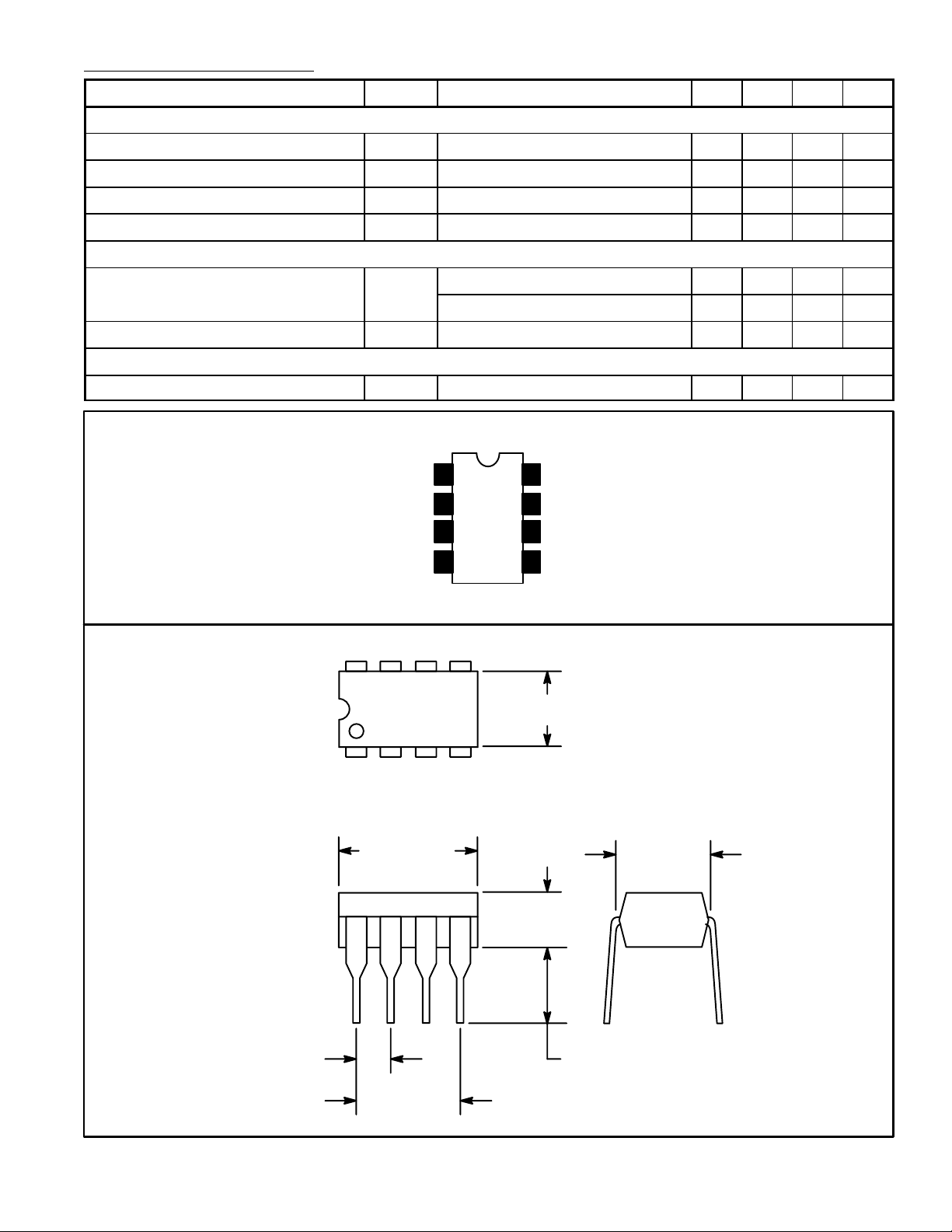
Pin Connection Diagram
1
2
3
4
Control Input
8
Q14 Input
7
Q14 Output
6
5
– – 100 mV
– – 15 µA
2 – 12 V
3 – 10 mA
.100 (2.54)
85
.260 (6.6)
14
.390 (9.9)
Max
.155
(3.93)
.300 (7.62)
.145 (3.68)
.300 (7.62)
 Loading...