

NTE NTE861 Datasheet

NTE861
Integrated Circuit
Quad, Normally Open, SPST JFET
Analog Switch w/Disable
Description:
The NTE861 is a monolithic combination of bipolar and JFET technology producing a one chip quad
JFET switch. A unique circuit technique is employed to maintain a constant resistance over the analog voltage range of ±10V. The input is designed to operate from minimum TTL levels, and switch
operation also ensures a break–before–make action.
Features:
D Analog signals are not loaded
D Constant “ON” resistance for signals up to ±10V and 100kHz
D Pin compatible with CMOS switches with the advantage of blow out free handling
D Small signal analog signals to 50MHz
D Break–before–make action
D High open switch isolation at 1.0MHz
D Low leakage in “OFF” state
D TTL, DTL, RTL compatibility
D Single disable pin opens all switches in package
This device operates from a ±15V supply and swings a ±10V analog signal. The JFET switches are
designed for applications where a dc to medium frequency analog signal needs to be controlled.
Absolute Maximum Ratings:
Positive Supply–Negative Supply (VCC –VEE) 36V. . . . . . . . . . . . . . . . . . . . . . . . . . . . . . . . . . . . . . . . .
Reference Voltage VEE ≤ VR ≤ V
Logic Input Voltage VR –4.0V ≤ VIN ≤ VR +6.0V. . . . . . . . . . . . . . . . . . . . . . . . . . . . . . . . . . . . . . . . . . .
Analog Voltage VEE ≤ VA ≤ VCC +6V; VA ≤ VEE +36V. . . . . . . . . . . . . . . . . . . . . . . . . . . . . . . . . . . . . . .
Analog Current IA < 20mA. . . . . . . . . . . . . . . . . . . . . . . . . . . . . . . . . . . . . . . . . . . . . . . . . . . . . . . . . . . . . .
Power Dissipation (Note 1) 500mW. . . . . . . . . . . . . . . . . . . . . . . . . . . . . . . . . . . . . . . . . . . . . . . . . . . . . . .
Operating Temperature Range 0° to 70°C. . . . . . . . . . . . . . . . . . . . . . . . . . . . . . . . . . . . . . . . . . . . . . . .
Storage Temperature –65° to 150°C. . . . . . . . . . . . . . . . . . . . . . . . . . . . . . . . . . . . . . . . . . . . . . . . . . . . . .
Typical Thermal Resistance, Junction–to–Ambient, R
Lead Temperature (Soldering, 10 seconds) +300°C. . . . . . . . . . . . . . . . . . . . . . . . . . . . . . . . . . . . . . . .
Note 1 For operating at high temperature this device must be derated based on a +100°C maximum
junction temperature and a thermal resistance of +150°C/W.
. . . . . . . . . . . . . . . . . . . . . . . . . . . . . . . . . . . . . . . . . . . . . . . . . . . . . .
thJA
CC
85°C/W. . . . . . . . . . . . . . . . . . . . . . . . . . . . .
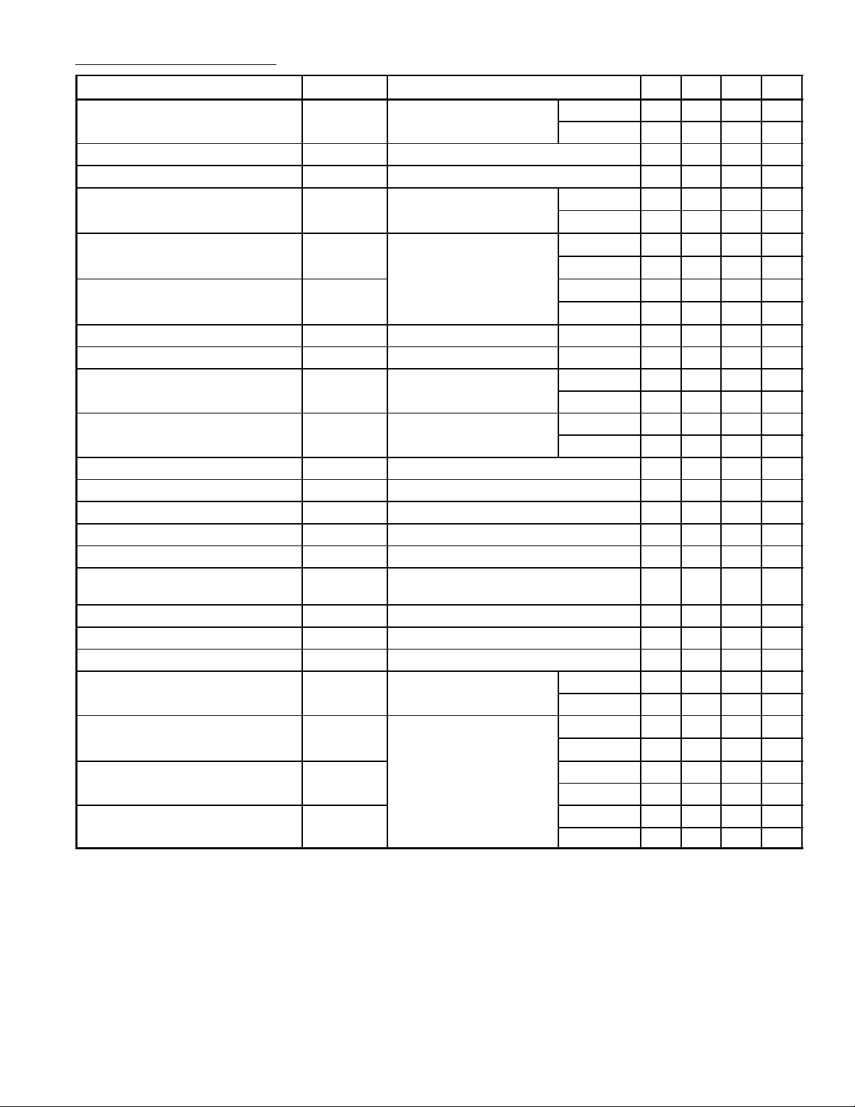
Electrical Characteristics: (Note 2)
Parameter Symbol Test Conditions Min Typ Max Unit
“ON” Resistance R
ON
“ON” Resistance Matching RON Match TA = +25°C – 10 50 Ω
Analog Range V
Leakage Current in “ON” Condition
Source Current in “OFF” Condition I
Drain Current in “OFF” Condition I
Logical “1” Input V oltage V
Logical “0” Input V oltage V
Logical “1” Input Current I
Logical “0” Input Current I
Delay Time “ON” t
Delay Time “OFF” t
I
S(ON)
I
D(ON)
S(OFF)
D(OFF)
INH
INL
ON
OFF
A
INH
INL
Break–Before–Make tON – t
Source Capacitance C
Drain Capacitance C
Active Source and Drain
Capacitance
“OFF” Isolation I
S(OFF)
D(OFF)
C
S(ON)
C
D(ON)
SO(OFF)
Crosstalk CT TA = +25°C, Note 3 – –65 – dB
Analog Slew Rate SR TA = +25°C, Note 4 – 50 – V/µs
Disable Current I
Negative Supply Current I
Reference Supply Current I
Positive Supply Current I
DIS
EE
R
CC
VA = 0, ID = 1mA TA = +25°C – 150 250 Ω
– 200 350 Ω
±10 ±11 – V
+ Switch “ON”,
+ VS = VD = ±10V
Switch “OFF”,
VS = +10V, VD = –10V
TA = +25°C – 0.3 10 nA
– 3 30 nA
TA = +25°C – 0.4 10 nA
– 3 30 nA
TA = +25°C – 0.1 10 nA
– 3 30 nA
2.0 – – V
– – 0.8 V
VIN = 5V TA = +25°C – 3.6 40 µA
– – 100 µA
VIN = 0.8V TA = +25°C – – 0.1 µA
– – 1.0 µA
VS = ±10V, TA = +25°C – 500 – ns
VS = ±10V, TA = +25°C – 90 – ns
OFFVS
= ±10V, TA = +25°C – 80 – ns
Switch “OFF”, VS = ±10V, TA = +2 5°C – 4.0 – pF
Switch “OFF”, VD = ±10V, TA = +2 5°C – 3.0 – pF
+
Switch “ON”, VS = VD = ±10V,
+
TA = +25°C
– 5.0 – pF
TA = +25°C, Note 3 – –50 – dB
Note 5 TA = +25°C – 0.6 1.5 mA
– 0.9 2.3 mA
All Switches “OFF”,
VS = ±10V
TA = +25°C – 4.3 7.0 mA
– 6.0 10.5 mA
TA = +25°C – 2.7 5.0 mA
– 3.8 7.5 mA
TA = +25°C – 7.0 9.0 mA
– 9.8 13.5 mA
Note 2. VCC = +15V, VEE = –15V, VR = 0V, and limits apply for –25°C ≤ TA ≤ +85°C unless otherwise
specified.
Note 3. These parameters are limited by the pin to pin capacitance of the package.
Note 4. This i s t he a nalog s ignal s lew r ate a bove w hic h t he s i gnal i s distorted as a r esult o f f inite internal
slew rates.
Note 5. All switches in the device are turned “OFF” by saturating a transistor at the disable node.
The delay times will be approximately equal to the tON or t
plus the delay introduced by
OFF
the external transistor.
 Loading...