

NTE NTE859 Datasheet

NTE859/NTE859SM
Integrated Circuit
Quad, Low Noise, JFET Input
Operational Amplifier
Description:
The NTE859 (14–Lead DIP) and NTE859SM (SOIC–14 Surface Mount) JFET–input operational amplifiers are low noise amplifiers with low noise input bias, offset currents, and fast slew rate. The low
harmonic distortion and low noise make these devices ideally suited as amplifiers for high–fidelity and
audio preamplifier applications. Each amplifier features JFET–inputs (for high input impedance)
coupled with bipolar output stages all integrated on a single monolithic chip.
Features:
D Low Power Consumption
D Wide Common–Mode and Differential Voltage Ranges
D Low Input Bias and Offset Currents
D Output Short–Circuit Protection
D Low Total Harmonic Distortion: 0.003% Typ
D Low Noise: Vn = 18nV√H
D High Input Impedance: JFET–Input Stage
D Internal Frequency Compensation
D Latch–Up Free Operation
D High Slew Rate: 13V/µs Typ
Ty p
Z
Absolute Maximum Ratings
Supply Voltage (Note 1), V
Supply Voltage (Note1), V
Differential Input Voltage (Note 2), V
Input Voltage Range (Note 1, Note 3),V
Duration of Output Short Circuit (Note 4),t
Power Dissipation (T
= +25°C), P
A
: (TA = 0 to +70°C unless otherwise specified)
(+) 18V. . . . . . . . . . . . . . . . . . . . . . . . . . . . . . . . . . . . . . . . . . . . . . . . . . . . . .
CC
(–) –18V. . . . . . . . . . . . . . . . . . . . . . . . . . . . . . . . . . . . . . . . . . . . . . . . . . . . .
CC
ID
IDR
S
D
±30V. . . . . . . . . . . . . . . . . . . . . . . . . . . . . . . . . . . . . . . . . . . . . . .
±15V. . . . . . . . . . . . . . . . . . . . . . . . . . . . . . . . . . . . . . . . . . .
Unlimited. . . . . . . . . . . . . . . . . . . . . . . . . . . . . . . . . . . . . . .
680mW. . . . . . . . . . . . . . . . . . . . . . . . . . . . . . . . . . . . . . . . . . . . . .
Derate Above 25°C 10mW/°C. . . . . . . . . . . . . . . . . . . . . . . . . . . . . . . . . . . . . . . . . . . . . . . . . . . . . .
Operating Ambient Temperature Range, T
Storage Temperature Range, T
stg
A
Lead Temperature (During Soldering, 1/16” from Case for 10sec), T
L
0° to +70°C. . . . . . . . . . . . . . . . . . . . . . . . . . . . . . . . . . . . .
–65° to +150°C. . . . . . . . . . . . . . . . . . . . . . . . . . . . . . . . . . . . . . . . . .
+260°C. . . . . . . . . . . . . . . . . .
Note 1. All voltage values, except differential voltages, are with reapect to the midpoint between
V
(+) and VCC(–).
CC
Note 2. Differential voltages are at the non–inverting input pin with respect to the inverting pin.
Note 3. The magnitude of the input voltage must never exceed the magnitude of the supply voltage
or 15V, whichever is less.
Note 4. The output may be shorted to GND or to either supply. Temperature and/or supply voltages
must be limited to ensure that the dissipation rating is not exceeded.
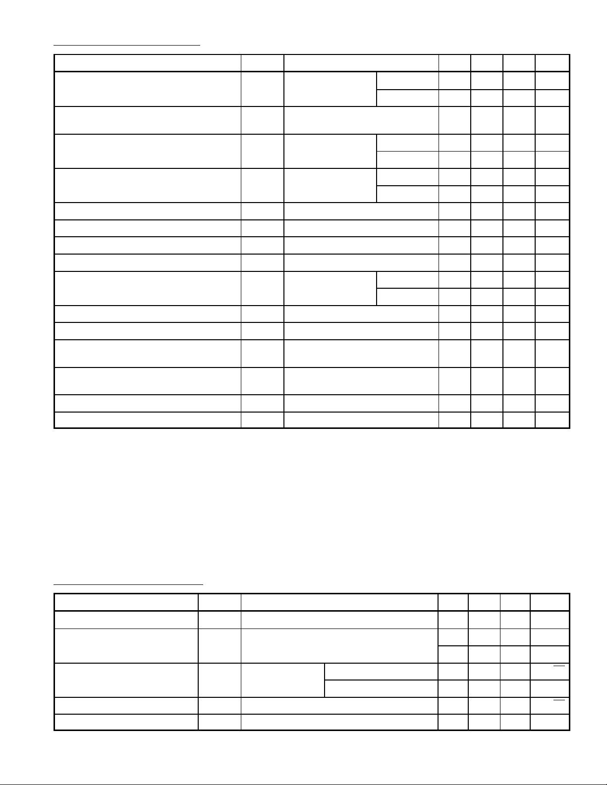
Electrical Characteristics: (VCC = ±15V, TA = 0 to+70°C unless otherwise specified)
Parameter Symbol Test Conditions Min Typ Max Unit
Input Offset Voltage V
VO = 0, RS = 50Ω
IO
TA = +25°C – 3 10 mV
– – 13 mV
Temperature Coefficient of Input Offset
αV
VO = 0, RS = 50Ω – 10 – µV/°C
IO
Voltage
Input Offset Current I
VO = 0, Note 6 TA = +25°C – 5 100 pA
IO
– – 2 nA
Input Bias Current I
VO = 0, Note 6 TA = +25°C – 30 200 pA
IB
– – 7 nA
Common–Mode Input Voltage Range V
Maximum Peak Output Voltage Range V
TA = +25°C ±11 ±12 – V
ICR
RL = 10kΩ, TA = +25°C ±12 ±13.5 – V
OM
RL = ≥10kΩ ±12 – – V
RL = ≥2kΩ ±10 ±12 – V
Large–Signal Differential Voltage A
VD
VO = ±10V,
Amplification RL ≥ 2kΩ
Unity–Gain Bandwidth B
Input Resistance r
TA = +25°C – 3 – MHz
1
TA = +25°C – 10
i
Common–Mode Rejection Ratio CMRR VIC = V
= +25°C
T
A
SupplyVoltage Rejection Ratio
CC
/∆VIO)
±
(∆V
Supply Current (Per Amplifier) I
k
SVR
CC
VCC = ±15V to ±9V, VO = 0,
= 50Ω, TA = +25°C
R
S
No Load, VO = 0, TA = +25°C – 1.4 2.5 mA
min, VO = 0, RS = 50Ω,
ICR
TA = +25°C 25 200 – V/mV
15 – – V/mV
12
– Ω
70 86 – dB
70 86 – dB
Crosstalk Attenuation Vo1/Vo2AVD = 100, TA = +25°C – 120 – dB
Note 5. All characteristics are measured under open–loop conditions with zero common–mode volt-
age unless otherwise specified.
Note 6. Input bias currents of a FET–input operational amplifier are normal junction reverse currents,
which are temperature sensitive. Pulse techniques must be used that will maintain the junction temperatures as close to the ambient temperature as is possible.
Operating Characteristics:
Parameter Symbol Test Conditions Min Typ Max Unit
Slew Rate at Unity Gain SR
Rise Time Overshoot Factor t
Equivalent Input Noise Voltage V
Equivalent Input Noise Current I
Total Harmonic Distortion THD V
(VCC = ±15V, TA = +25°C unless otherwise specified)
VI = 10V, RL = 2kΩ, CL = 100pF
VI = 10V, RL = 2kΩ, CL = 100pF
r
n
n
I L L
RS = 100Ω f = 1kHz – 18 – nV/√Hz
f = 10Hz to 10kHz – 4 – µV
RS = 100Ω, f = 1kHz – 0.01 – pA/√Hz
= 10V, RS ≤ 1kΩ, RL ≥ 2kΩ, f = 1kHz – 0.003 – %
O(rms)
8 13 – V/µs
– 0.1 – µs
– 10 – %
 Loading...