

NTE NTE855 Datasheet

NTE855
Integrated Circuit
Color TV Video Monitor
Description:
The NTE855 is an integrated circuit in a 14–Lead DIP type package used to generate an RF TV signal
from baseband color–difference and luminance signals. This device contains a chroma subcarrier
oscillator, a lead and lag network, a quasi–quadrature suppressed carrier DSB chroma modulator,
an RF oscillator and modulator, and an LSTTL compatible clock driver with adjustable duty cycle. The
NTE855 may be used as a general–purpose modulator with a variety of video signal generating devices such as video games, test equipment, video tape recorders, etc.
Features:
D Single 5V Supply Operation for NMOS and TTL Compatibility
D Minimal External Components
D Sound Carrier Addition Capability
D Modulates Channel 3 or 4 Carrier with Encoded Video Signal
D Low Power Dissipation
D Linear Chroma Modulators for High Versatility
D Composite Video Signal Generation Capability
D GND–Referenced Video Prevents Overmodulation
Absolute Maximum Ratings:
Supply Voltage, V
Power Dissipation, P
CC
D
(TA = +25°C unless otherwise specified)
1.25W. . . . . . . . . . . . . . . . . . . . . . . . . . . . . . . . . . . . . . . . . . . . . . . . . . . . . . . . . . . .
Derate Above 25°C 13mW/°C. . . . . . . . . . . . . . . . . . . . . . . . . . . . . . . . . . . . . . . . . . . . . . . . . . . . . .
Operating Junction Temperature, T
J
Operating Ambient Temperature Range, T
Storage Temperature Range, T
stg
opr
–65° to +150°C. . . . . . . . . . . . . . . . . . . . . . . . . . . . . . . . . . . . . . . . . .
+150°C. . . . . . . . . . . . . . . . . . . . . . . . . . . . . . . . . . . . . . . . . . . . . . .
0° to +70°C. . . . . . . . . . . . . . . . . . . . . . . . . . . . . . . . . . . .
Recommended Operating Conditions:
Supply Voltage, V
CC
Luma Input Voltage, Sync Tip 1V. . . . . . . . . . . . . . . . . . . . . . . . . . . . . . . . . . . . . . . . . . . . . . . . . . . . . . . . .
Luma Input Voltage, Peak White 350mV. . . . . . . . . . . . . . . . . . . . . . . . . . . . . . . . . . . . . . . . . . . . . . . . . .
Color Reference Voltage 1.5V. . . . . . . . . . . . . . . . . . . . . . . . . . . . . . . . . . . . . . . . . . . . . . . . . . . . . . . . . . .
Color A, B Input Voltage range 1V to 2V. . . . . . . . . . . . . . . . . . . . . . . . . . . . . . . . . . . . . . . . . . . . . . . . . . .
8V. . . . . . . . . . . . . . . . . . . . . . . . . . . . . . . . . . . . . . . . . . . . . . . . . . . . . . . . . . . . . . . . .
5V. . . . . . . . . . . . . . . . . . . . . . . . . . . . . . . . . . . . . . . . . . . . . . . . . . . . . . . . . . . . . . . . .
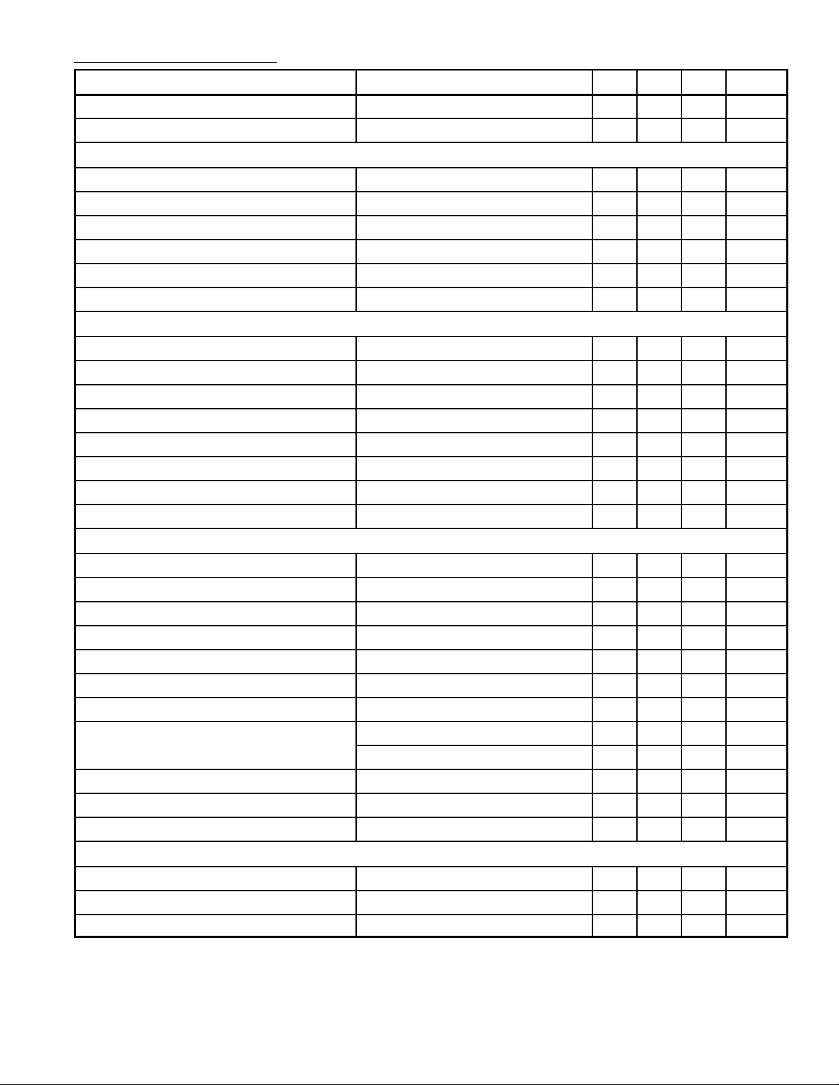
Electrical Characteristics: (VCC = 5V, TA = +25°C unless otherwise specified)
Parameter Test Conditions Min Typ Max Unit
Operating Supply Voltage 4.75 5.00 5.25 V
Supply Current – 25 – mA
Chroma Oscillator/Clock Driver (Measured at Pin1 unless otherwise specified)
Output Voltage, LOW – – 0.4 V
Output Voltage, HIGH 2.4 – – V
Rise Time V1 = 0.4V to 2.4V – – 50 ns
Fall Time V1 = 2.4V to 0.4V – – 50 ns
Duty Cycle Adjustment Range V3 = 5V, Measured at V1 = 1.4V 70 – 30 %
Inherent Duty Cycle No connection to Pin3 – 50 – %
Chroma Modulator (V5 = V6 = V7 = 1.5V unless otherwise specified)
Input Common–Mode Voltage Range Pin5, Pin6, Pin7 0.8 – 2.3 V
Oscillator Feedthrough Measured at Pin8 – 15 31 mV
(p–p)
Modulation Angle (V7 =2V) – (V5 = 2V) 85 100 115 deg
Conversion Gain V8/(V7 – V6); V8/(V5 – V6) – 0.6 – V
(p–p)
Input Current Pin5, Pin6, Pin7 – – –20 µA
Input Resistance Pin5, Pin6, Pin7 100 – – kΩ
Input Capacitance Pin5, Pin6, Pin7 – – 5 pF
Chroma Modulator Linearity V5 = 1V to 2V, V7 = 1V to 2V – 40 – %
RF Modulator
Luma Input Dynamic Range Pin9 0 – 1.5 V
RF Output Voltage f = 67.25MHz, V9 = 1V – 15 – mV
rms
Luma Conversion Gain V9 = 0.1V to 1.oV – 0.8 – V/V
Chroma Conversion Gain V10 = 1.5V
Chroma Linearity Pin12, V10 = 1.5V
Luma Linearity Pin12, V9 = 0 to 1.5V
, V9 = 1V – 0.95 – V/V
p–p
p–p
p–p
– 1 – %
– 2 – %
Input Current Pin9 – – –20 µA
Input Resistance Pin9 – 800 – Ω
Pin10 100 – – kΩ
/V
Input Capacitance Pin9, Pin10 – – 5 pF
Residual 920kHz Measured at Pin12, Note 1 – 50 – dB
Output Current Pin12, V9 = 0 – 1 – mA
Temperature Characteristics (VCC = 5V, TA = 0° to +70°C, IC only)
Chroma Oscillator Deviation fo = 3.579545MHz – ±50 – Hz
RF Oscillator Deviation fo = 67.25MHz – ±250 – kHz
Clock Drive Duty Stability ±5 – – %
Note 1. V9 = 1 V, VC = 300mV
@ 3.58MHz, VS = 250mV
p–p
@ 4.5MHz, Source Impedance = 75Ω.
p–p
 Loading...