

NTE NTE851 Datasheet

NTE851
Integrated Circuit
VHF/UHF Prescaler
Description:
The NTE851 is an integrated circuit prescaler in a 14–Lead DIP type package intended for use in TV
frequency synthesis tuning systems over an input frequency range of 90 to 1000MHz. It performs
division by 256 in he UHF mode and division by 64 in the VHF mode.
The mode of operation can be selected by means of the bandswitch and the separate UHF and VHF
input pins provided. The output is a complementary emitter–coupled stage with controlled slew rate
for harmonic suppression.
All input pins should be AC coupled to the appropriate input signal source. Because of high sensitivity,
unbuffered coupling from the local oscillator is possible in most cases. In the UHF mode, which is
activated by applying a high level to the bandswitch input pin, all eight divider stages are operative,
resulting in division by 256. In the VHF mode, activated by a low level at the VHF input pin, two divider
stages are bypassed, resulting in division by 64. As a result, approximately the same range of output
frequencies are generated fo both the UHF and VHF TV bands. An internal amplifier/multiplexer provides this control while isolating both inputs and amplifying the VHF signal. In addition, hrmonic output
is reduced above 40MHz by limiting output signal rise and fall times and maintaining a balanced load.
Features:
D Broadband Operation: 90 to 1000MHz
D High Sensitivity
D Standard 5V Power Supply
D Dual Mode Operation: VHF/UHF
D Complementary ECL Outputs
D Independent VHF & UHF Input Pins
Absolute Maximum Ratings:
DC Supply Voltage 5.5V. . . . . . . . . . . . . . . . . . . . . . . . . . . . . . . . . . . . . . . . . . . . . . . . . . . . . . . . . . . . . . . .
DC bandswitch Voltage 20V. . . . . . . . . . . . . . . . . . . . . . . . . . . . . . . . . . . . . . . . . . . . . . . . . . . . . . . . . . . . .
RMS Input Voltage 500mV. . . . . . . . . . . . . . . . . . . . . . . . . . . . . . . . . . . . . . . . . . . . . . . . . . . . . . . . . . . . . .
Device Dissipation (T
Derate Linearly Above 70°C 7.5mW/°C. . . . . . . . . . . . . . . . . . . . . . . . . . . . . . . . . . . . . . . . . . . . .
Operating Ambient Temperature Range 0° to +70°C. . . . . . . . . . . . . . . . . . . . . . . . . . . . . . . . . . . . . . . .
Storage Temperature Range –55° to +150°C. . . . . . . . . . . . . . . . . . . . . . . . . . . . . . . . . . . . . . . . . . . . . . .
Lead Temperature (During Soldering, 1/16” from case, 10sec max) +265°C. . . . . . . . . . . . . . . . . . . .
≤ +70°C) 600mW. . . . . . . . . . . . . . . . . . . . . . . . . . . . . . . . . . . . . . . . . . . . . . . . . .
A
Electrical Characteristics: (TA = +25°C, V+ = 5V, V– = 0 unless otherwise specified)
Parameter Symbol Test Conditions Min Typ Max Unit
Supply Current I+ Pin1 and Pin2 30 60 90 mA
UHF Bandswitch Input Voltage V
VHF Bandswitch Input Voltage V
UHF Bandswitch Input Current I
VHF Bandswitch Input Current I
BH
BL
High Level 2.4 – – V
BH
Low Level – – 0.8 V
BL
VBH = 20V – – 0.5 mA
VBL = 0 – – –1 mA
UHF Sensitivity Level Input Voltage VIN(U) fIN = 450 to 950MHz, f
VHF Sensitivity Level Input Voltage VIN(V) fIN = 90 to 275MHz, f
Output Voltage V
Output Voltage Rise and Fall Time tr, t
Pin4 or Pin5 0.65 1.0 – V
O
f
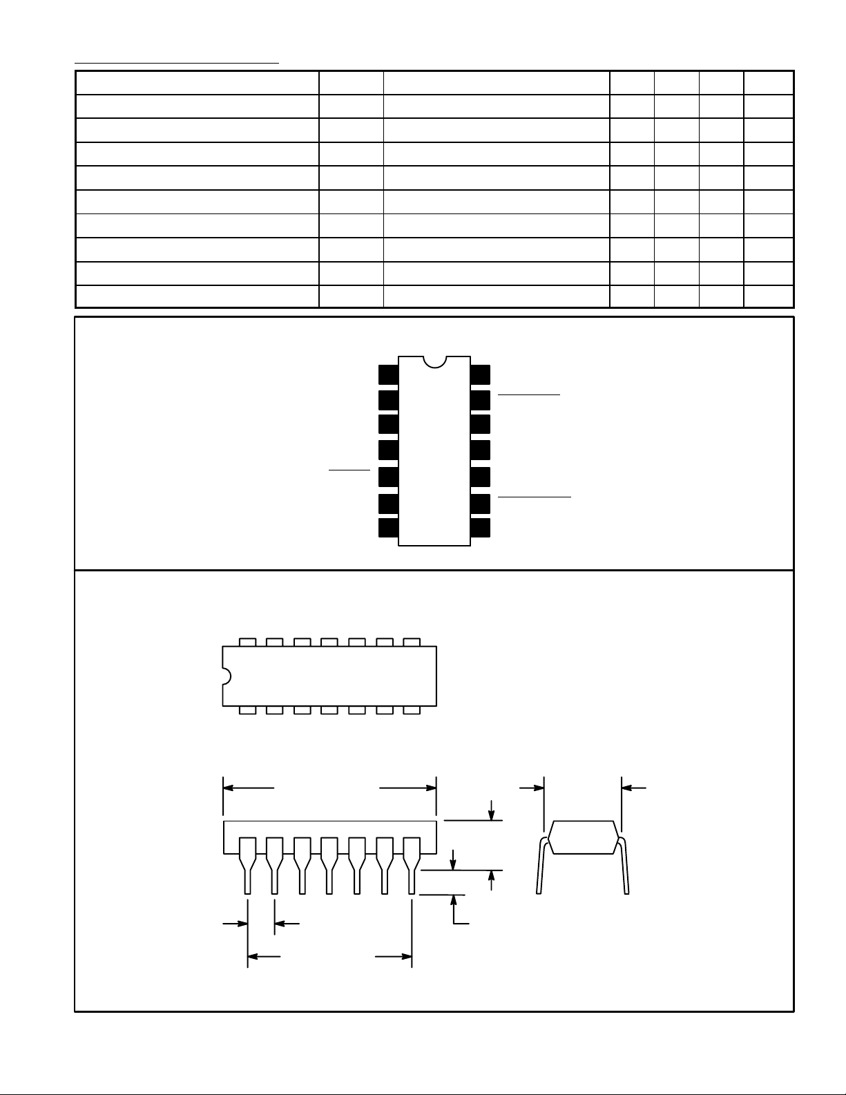
Pin Connection Diagram
V(+) 1
V(+) 2
Bandswitch Input
Output
Output
V(–) 1
1
2
3
4
5
6N.C.
7
VHF Input
14
13
VHF Input
12
N.C.
11 N.C.
10
UHF Output
UHF Output
9
8
V(–) 2
= fIN/256 – – 80 mV
OUT
= fIN/64 mV
OUT
– 70 – ns
rms
rms
P–P
14 8
17
.785 (19.95)
Max
.200 (5.08)
Max
.100 (2.45) .099 (2.5) Min
.600 (15.24)
.300
(7.62)
 Loading...