

NTE NTE832SM, NTE834SM, NTE834 Datasheet

NTE832 & NTE832SM
Integrated Circuit
Tone Decoder
Description:
The NTE832 and NTE832SM are general purpose tone decoders designed to provide a saturated
transistor switch to GND when an input signal is present within the passband. The circuit consists
of an I and Q detector driven by a voltage controlled oscillator which determines the center frequency
of the decoder. External components are used to independently set center frequency, bandwidth, and
output delay.
Features:
D Logic Compatible Output with 100mA Current Sinking Capability
D Bandwidth Adjustment from 0 to 14%
D Inherent Immunity to False Signals
D High Stable Center Frequency
D High Rejection of Out–Of–Band Signals and Noise
D Center Frequency Adjustable from 0.01Hz to 500kHz
D Frequecny Range Adjustable over 20:1 range by an External Resistor
D Available in Standard 8–Lead DIP (NTE832) and Surface Mount SOIC–8 (NTE832SM)
Applications:
D Touch Tone Decoder
D Precision Oscillator
D Frequency Monitoring and Control
D Wide Band FSK Demodulation
D Communications Paging Decoders
D Carrier Current Remote Controls
D Ultrasonic Controls (Remote TV, etc.)
Absolute Maximum Ratings:
Operating Voltage, V
Input Voltage, V
Output Voltage, V
Power Dissipation (Note 1), P
CC
IN
O
D
Operating Temperature Range, T
Storage Temperature Range, T
stg
opr
–10V to VCC +0.5V. . . . . . . . . . . . . . . . . . . . . . . . . . . . . . . . . . . . . . . . . . . . . . . . . . . .
0° to +70°C. . . . . . . . . . . . . . . . . . . . . . . . . . . . . . . . . . . . . . . . . . .
–65° to +150°C. . . . . . . . . . . . . . . . . . . . . . . . . . . . . . . . . . . . . . . . . .
10V. . . . . . . . . . . . . . . . . . . . . . . . . . . . . . . . . . . . . . . . . . . . . . . . . . . . . . . . . . . . .
15V. . . . . . . . . . . . . . . . . . . . . . . . . . . . . . . . . . . . . . . . . . . . . . . . . . . . . . . . . . . . . . . . .
300mW. . . . . . . . . . . . . . . . . . . . . . . . . . . . . . . . . . . . . . . . . . . . . . . . . . . .
Note 1. The maximum junction temperature of these devices is +100°C. For operating at elevated
temperatures, devices m ust b e d erated o n a thermal resistance o f + 187°C/W, junction–to–ambient.
Electrical Characteristics: (VCC = 5V, TA = +25°C, unless otherwise specified)
Parameter Test Conditions Min Typ Max Unit
Power Supply Voltage 4.75 5.00 9.00 V
Power Supply Current, Quiescent RL = 20kΩ – 7 10 mA
Power Supply Current, Activated – 12 15 mA
Quiescent Power Dissipation – 35 – mW
Input Resistance 15 20 25 kΩ
Smallest Detectable Input Voltage IL = 100mA, fi = f
Largest No Output Input Voltage IC = 100mA, fi = f
Largest Simultaneous Outband Signal to Inband
RL = 20kΩ – +6 – dB
o
o
Signal Ratio
Minimum Input Signal to Widband Noise Ratio Bn = 140kHz – –6 – dB
Largest Detection Bandwidth 10 14 18 % of f
Largest Detection Bandwidth Skew – 2 3 % of f
Largest Detection Bandwidth with Variation with
Temperature
Largest Detection bandwidth with Variation with
4.75V to 6.75V – ±1 ±5 %/V
Supply Voltage
Highest Center Frequency RL = 20kΩ 100 500 – kHz
Center Frequency Stability 0° < TA , +70°C – 35±60 – ppm/°C
–55° < TA < +125°C – 35±140 – ppm/°C
Center Frequency Shift with Supply Voltage 4.75V to 6.75V – 0.4 2.0 %/V
Fastest ON–OFF Cycling Rate – fo/20 –
Output Leakage Current V8 = 15V – 0.01 25.0 µA
Output Saturation Voltage ei = 25mV, I8 = 30mA – 0.2 0.4 V
ei = 25mV, I8 = 100mA – 0.6 1.0 V
Output Fall Time – 30 – ns
Output Rise Time – 150 – ns
– 20 25 mV
10 15 – mV
– ±0.1 ±0.5 %/°C
rms
rms
o
o
Output Filter
Loop Filter12
Input
V
CC
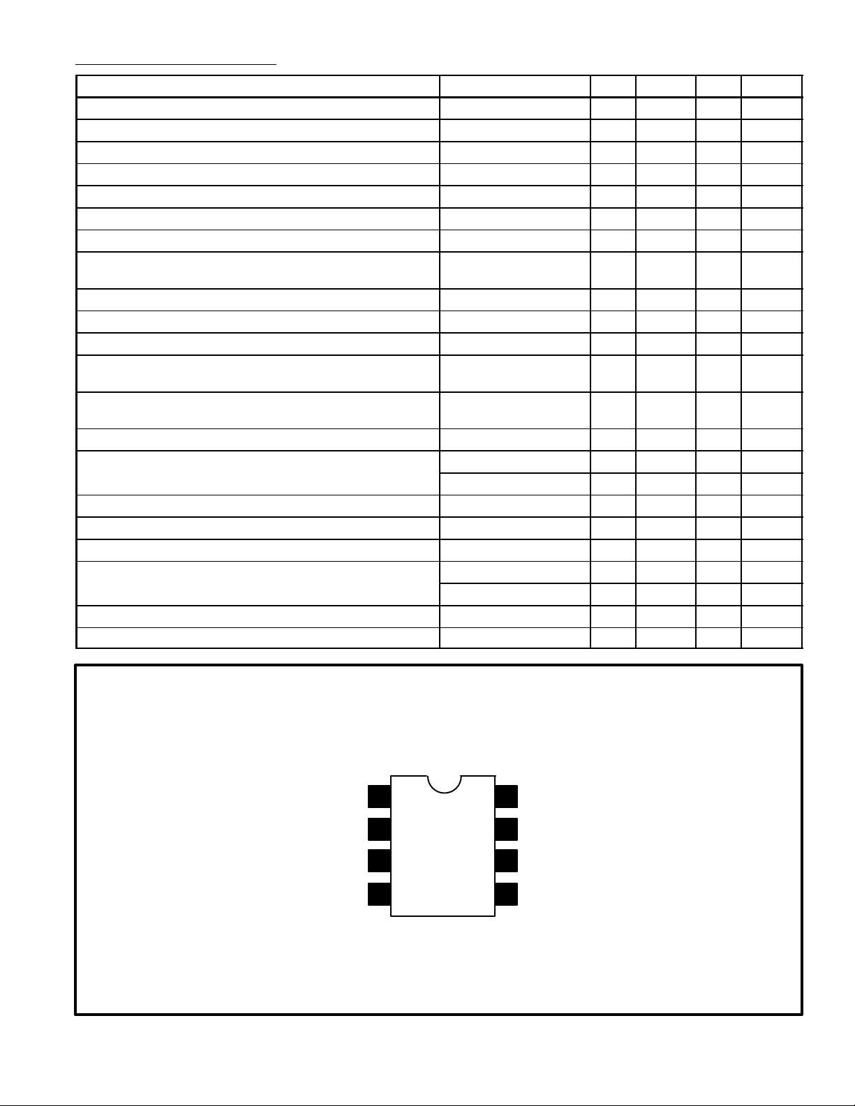
Pin Connection Diagram
8
7
3
4
6
5
Output
GND
Timing Capacitor
Timing Resistor
 Loading...