

NTE NTE828 Datasheet

NTE828
Integrated Circuit
Audio Power Amp, 1.5W
Description:
The NTE828 is an audio amplifier in a 14–Lead DIP type package designed for use in medium power
consumer applications. The gain is internally set to 20 to keep external part count low , but the addition
of an external resi stor a nd capaci tor betw een Pi n2 and P in6 w ill increase the gain to any v alue u p to 200.
The i nputs a re g round r efer enced w hi le t he o utput i s a utomati cally b iased t o o ne h alf t he s upply v ol tage.
Features:
D Minimum External Parts
D Wide Supply Voltage Range
D Ground Referenced Input
D Excellent Supply Rejection
D Variable Voltage Gain
D Self–Centering Output Quiescent Voltage
D Low Distortion
D Low Voltage Operation, 4V
Applications:
D AM–FM Radio Amplifiers
D Intercoms
D TV Sound Systems
D Portable Tape Player Amplifiers
D Power Converters
D Lamp Drivers
D Ultrasonic Drivers
D Line Drivers
D Small Servo Drivers
Absolute Maximum Ratings:
Supply Voltage, V
Package Dissipation (Note 1), P
Input Voltage, V
Operating Junction Temperature, T
Operating Temperature Range, T
Storage Temperature Range, T
S
D
IN
J
opr
stg
Lead Temperature (During Soldering, 10sec), T
0° to +70°C. . . . . . . . . . . . . . . . . . . . . . . . . . . . . . . . . . . . . . . . . . .
–65° to +150°C. . . . . . . . . . . . . . . . . . . . . . . . . . . . . . . . . . . . . . . . . .
L
22V. . . . . . . . . . . . . . . . . . . . . . . . . . . . . . . . . . . . . . . . . . . . . . . . . . . . . . . . . . . . . . . . .
8.3W. . . . . . . . . . . . . . . . . . . . . . . . . . . . . . . . . . . . . . . . . . . . . . . . . . .
±0.4V. . . . . . . . . . . . . . . . . . . . . . . . . . . . . . . . . . . . . . . . . . . . . . . . . . . . . . . . . . . . . . . .
+150°C. . . . . . . . . . . . . . . . . . . . . . . . . . . . . . . . . . . . . . . . . . . . . . .
+300°C. . . . . . . . . . . . . . . . . . . . . . . . . . . . . . . . . . . .
Note 1 Pin3, Pin4, Pin5, Pin10, Pin11, and Pin12 at +25°C. Derate at 15°C/W above +25°C case.
Electrical Characterisitics: (TA = 25°C unless otherwise specified)
Parameter Symbol Test Conditions Min Typ Max Unit
Operating Supply Voltage V
Quiescent Current I
Output Power P
Voltage Gain A
Bandwidth BW VS = 12V, Pin2 and Pin6 Open – 300 – kHz
Total Harmonic Distortion THD VS = 12V, RL = 8Ω, P
Power Supply Rejection Ratio PSRR VS = 12V, f = 1kHz, C
Input Resistance R
Input Bias Current I
S
Q
OUT
V
IN
BIAS
VS = 16V, VIN = 0 – 20 35 mA
R1 = R2 = 180Ω,
THD = 10%, Note 2
VS = 12V, f = 1khz, 23 26 30 dB
10µF from Pin2 to Pin6 – 46 – dB
OUT
Pin2 and Pin6 Open
Pin2 and Pin6 Open, Referred to Output, Note 3
VS = 12V, Pin7 and Pin8 Open – 250 – nA
VS = 12V, RL = 8Ω 1.5 2.2 – W
VS = 6V, RL = 4Ω 0.6 0.8 – W
= 500mW, f = 1kHz,
BYPASS
= 10µF,
5 – 18 V
– 0.1 1.0 %
– 50 – dB
10 50 – kΩ
Note 2 The amplifier should be in high gain for full swing on higher supplies due to input voltage li-
mitations.
Note 3 If load and bypass capacitor are returned to VS rather than ground, PSRR is typically 30dB.
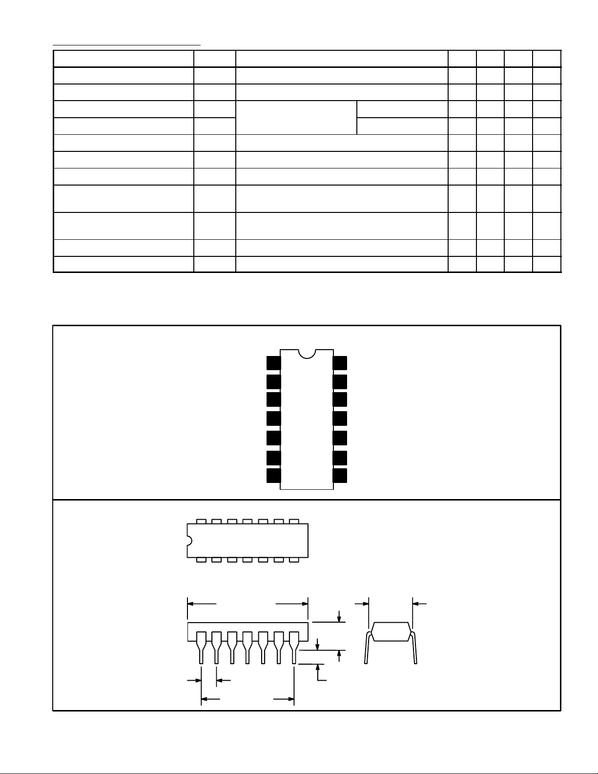
Pin Connection Diagram
Bypass
Gain
GND
GND
GND
14 8
17
.785 (19.95)
Max
1
2
3
4
5
6Gain
7(–) Input
14
V
13
V
GND
12
11 GND
10 GND
9 Bootstrap
8 (+) Input
.200 (5.08)
Max
S
out
.300
(7.62)
.100 (2.45)
.600 (15.24)
.099 (2.5) Min
 Loading...