

NTE NTE825 Datasheet

NTE825
Integrated Circuit
Battery Operated Audio Amp
Description:
The NTE825 amplifier is an integrated circuit in a 14–Lead DIP type package optimized for 6V , 7.5V,
and 9V operation into low impedance loads. The gain is internally set at 20 to keep the external part
count low, but the addition of an external resistor and capacitor between Pin2 and Pin6 will increase
the gain to any value up to 200. The inputs are ground referenced while the output is automatically
biased to one half the supply voltage.
Features:
D Battery Operation
D 1W Output Power
D Excellant Supply Rejection
D Low Distortion
Applications:
D AM–FM Radio Amplifiers
D Portable Tape Player Amplifiers
D TV Sound Systems
Absolute Maximum Ratings: (Note 1)
Supply Voltage, V
Power Dissipation, P
Input Voltage, V
Storage Temperature Range, T
Operating Temperature Range, T
Junction Temperature, T
S
D
I
stg
opr
J
–65° to +150°C. . . . . . . . . . . . . . . . . . . . . . . . . . . . . . . . . . . . . . . . . .
0° to +70°C. . . . . . . . . . . . . . . . . . . . . . . . . . . . . . . . . . . . . . . . . . .
Lead Temperature (During Soldering, 10 seconds), TL +300°C. . . . . . . . . . . . . . . . . . . . . . . . . . . . . . .
Note 1. Pins 3, 4, 5, 10, 11, 12 at TC = +25°C. Derate at 15°C/W above TC = +25°C.
10V. . . . . . . . . . . . . . . . . . . . . . . . . . . . . . . . . . . . . . . . . . . . . . . . . . . . . . . . . . . . . . . . .
8.3W. . . . . . . . . . . . . . . . . . . . . . . . . . . . . . . . . . . . . . . . . . . . . . . . . . . . . . . . . . . . .
±0.4V. . . . . . . . . . . . . . . . . . . . . . . . . . . . . . . . . . . . . . . . . . . . . . . . . . . . . . . . . . . . . . . . .
+150°C. . . . . . . . . . . . . . . . . . . . . . . . . . . . . . . . . . . . . . . . . . . . . . . . . . . . . . . . .
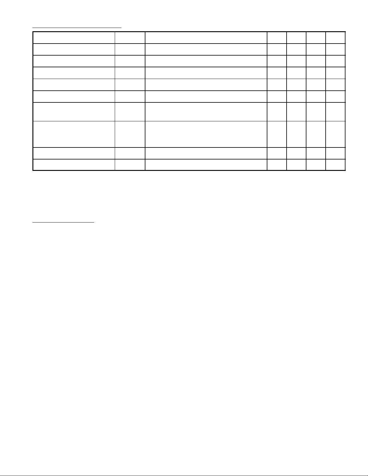
Electrical Characteristics: (TA = 25°C unless otherwise specified)
Parameter Symbol Test Conditions Min Typ Max Unit
Operating Supply Voltage V
Quiescent Current I
Output Power P
Voltage Gain A
Bandwidth BW VS = 6V, Pin2 and Pin6 Open – 46 – kHz
Total Harmonic Distortion THD VS = 6V, RL = 4Ω, P
Power Supply Rejection
Ratio
Input Resistance R
Input Bias Current I
S
Q
OUT
PSRR VS = 6V, f = 1kHz, C
BIAS
VS = 6V, RL = 4Ω, THD = 10%, Note 2 – 10 20 mA
VS = 6V, RL = 4Ω, THD = 10%, Note 2 0.8 1.0 – W
VS = 6V, f = 1kHz 10µF from Pin2 to Pin6 23 26 30 dB
V
f = 1kHz, Pin2 and Pin6 Open
Pin2 and Pin6 Open, Referred to Output,
Note 3
IN
VS = 6V, Pins 7 and 8 Open – 250 – mA
= 500mW,
OUT
BYPASS
= 10µF,
4 – 9 V
– 0.2 1 %
– 50 – dB
10 50 – kΩ
Note 2. If oscillation exists under some load conditions, add a 2.7Ω and 0.05µF series network from
Pin13 to GND.
Note 3. If load and bypass capacitor are returned to VS rather than GND, PSRR is typically 30dB.
Application Hints:
Gain Control
To make the NTE825 a more versatile amplifier , two pins (Pin2 and Pin6) are provided for gain
control. With Pin2 and Pin6 open, the gain is 20 (26dB). If a capacitor is put from Pin2 to Pin6,
the gain will go up to 200 (46dB). If a resistor is placed in series with the capacitor, the gain
can be set to any value from 20 to 200. A 10µf Electrolytic with positive to Pin6 is a usual value.
Additional external components can be placed in parallel with the internal feedback resistors
to tailor the gain and frequency response for inidividual applications. For example, a series
RC from Pin6 to Pin13 (paralleling the internal 15kΩ resistor) yields 6dB effective bass boost
if R ≅ 15kΩ and Pin2 is open. If Pin2 and Pin6 are bypassed, then R as low as 2kΩ can be
used. This restriction is because the amplifier is only compensated for closed–loop gains
greater than 9V/V.
Input Biasing
When using NTE825 with higher gains (bypassing the internal 1.35kΩ resistor between Pin2
and Pin6) it is necessary to bypass the unused input, preventing degradation of gain and possible instabilities. This is done with a 0.1µF capacitor or a short to GND depending on the DC
source resistance on the driven input.
 Loading...