

NTE NTE8212 Datasheet

NTE8212
Integrated Circuit
Schottky, 8–Bit Input/Output Port
Description:
The NTE8212 input/output port is an integrated circuit in a 24–Lead DIP type package and consists
of an 8–bit latch with three–state output buffers along with control and device selection logic. Also
included is a service request f lip–fl op f or t he c ontrol a nd g eneration o f i nterrupts t o t he m icroprocessor.
Features:
D Fully Parallel 8–Bit Data Register and Buffer
D Service Request Flip–Flop for Interrupt Generation
D Low Input Load Current: 0.25mA Max
D Three State Outputs
D Outputs Sink 15mA
D 3.65V Output High Voltge for Direct Interface to 8080A Processor
D Asynchronous Register Clear
D Replaces Buffers, Latches and Multiplexers in Microcomputer Systems
D Reduces System Package Count
Absolute Maximum Ratings: (TA = +25°C, Note 1 unless otherwise specified)
All Output or Supply Voltages –0.5V to +7V. . . . . . . . . . . . . . . . . . . . . . . . . . . . . . . . . . . . . . . . . . . . . . . .
All Input Voltages –1.0V to +5.5V. . . . . . . . . . . . . . . . . . . . . . . . . . . . . . . . . . . . . . . . . . . . . . . . . . . . . . . .
Output Currents 125mA. . . . . . . . . . . . . . . . . . . . . . . . . . . . . . . . . . . . . . . . . . . . . . . . . . . . . . . . . . . . . . . . .
Operating Temperature Range 0° to +70°C. . . . . . . . . . . . . . . . . . . . . . . . . . . . . . . . . . . . . . . . . . . . . . . .
Storage Temperature Range –65° to +150°C. . . . . . . . . . . . . . . . . . . . . . . . . . . . . . . . . . . . . . . . . . . . . . .
Note 1. Stress above those listed under “Absolute Maximum Ratings” may cause permanent dam-
age to the device. This is a stress rating only and functional operation of the device at these
or any other conditions above those indicated in the operational sections of this specification
is not implied. Exposure to absolute maximum rating conditions for extended periods may
affect device reliability.
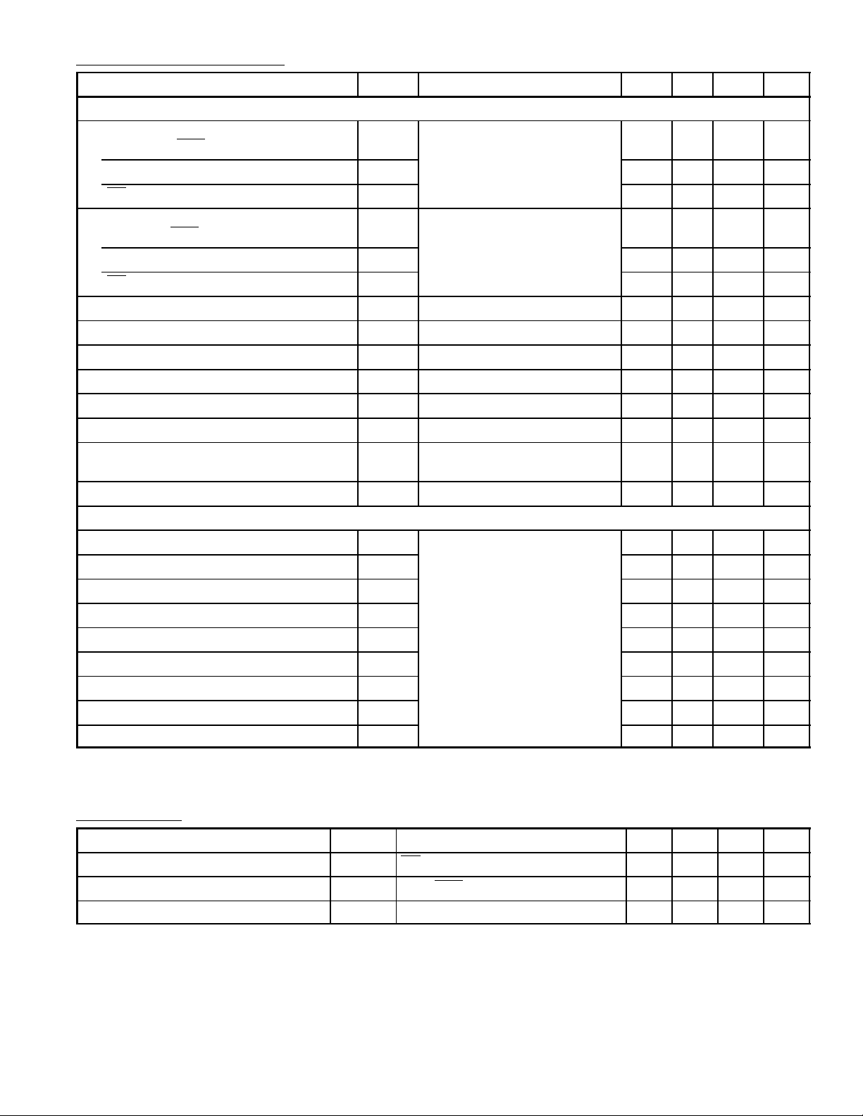
Electrical Characteristics: (TA = 0° to +70°C, VCC = 5V ±5% unless otherwise specified)
Parameter Symbol Test Conditions Min Typ Max Unit
DC Characteristics
Input Load Current
STB, DS
MD Input |IL2| – – –0.75 mA
DS1 Input |IL3| – – –1.0 mA
Input Leakage Current
STB, DS, CLR, DI1 – DI8 Inputs |IH1| VR = 5.25V – – 10 µA
MD Input |IH2| – – 30 µA
DS1 Input |IH3| – – 40 µA
, CLR, DI1 – DI8 Inputs |IL1| VF = 0.45V – – –0.25 mA
2
Input Forward Voltge Clamp V
Input “Low” V oltage V
Input “High” V oltage V
Output “Low” Voltage V
Output “High” V oltage V
IC = –5mA – – –1.0 V
C
IL
IH
OLIOL
OHIOH
= 15mA – – 0.48 V
= –1mA 3.65 – – V
– – 0.85 V
2.0 – – V
Short Circuit Output Current IO5 VO = 0V, VCC = 5V –15 – –75 mA
Output Leakage Current, High Impedance
I
VO = 0.45V/5.25V – – 20 µA
O
State (DO0 – DO8)
Power Supply Current I
CC
– – 130 mA
AC Characteritics
Pulse Width t
pw
Data to Output Delay t
Write Enable to Output Delay t
data Setup Time t
we
set
Data Hold Time t
Reset to Output Delay t
Set to Output Delay t
Output Enable/Disable Time (Note 2) te/t
Clear to Output Delay t
Input Pulse Amplitude = 2.5V,
Input Rise & Fall Times = 5ns,
pd
Between 1V and 2V
Between 1V and 2V
Measurement made
at 1.5V with 15mA and 30pF
Test Load
h
r
s
d
c
30 – – ns
– – 30 ns
– – 40 ns
15 – – ns
20 – – ns
– – 40 ns
– – 30 ns
– – 45 ns
– – 55 ns
Note 2. R1 = 300Ω/10KΩ; R2 = 600Ω/1KΩ
Capacitance: (TA = +25°C, VCC = 5V, V
Parameter Symbol Test Conditions Min Typ Max Unit
Input Capacitance C
Input Capacitance C
Output Capacitance C
IN
IN
OUT
= 2.5V, f = 1MHz, Note 3 unless otherwise specified)
BIAS
DS1, MD – – 12 pF
DS2, CLR, STB, DI1 – DI
DO1 – DO
8
8
Note 3. This parameter is periodically sampled and not 100% tested.
– – 9 pF
– – 12 pF
 Loading...