

NTE NTE821 Datasheet
NTE821
Integrated Circuit
TV Chroma Demodulator
Description:
Specifically designed to match advances in color picture tube phosphors, the NTE821 is a monolithic
silicon integrated circuit in a 14–Lead DIP type package and consists of three output amplifiers, a
new resistor matrix, two double–balanced chroma demodulators, and a very stable bias circuit. When
used with the NTE714 subcarrier regeneration system and the NTE715 chroma amplifier, this device
completes the typical three–block chroma system. Alternatively, the NTE821 chroma demodulator
can be used with the NTE738 chroma processor to form a complete two–block chroma system.
The output amplifiers are specifically designed to meet the low impedance, short–circuit protected
driving requirements of high–level color output amplifiers. Internal ripple filter capacitors greatly reduce the high–frequency components of demodulation and thereby extend the output voltage swing
capability of the output stages and at the same time eliminates the need for external output filtering
components.
Features:
D Output Short–Circuit Protection
D Excellent Subcarrier Rejection
D 600mV Maximum Offset Voltage
D 2mV/°C Typical Temperature Stability
D Good Chroma Sensitivity
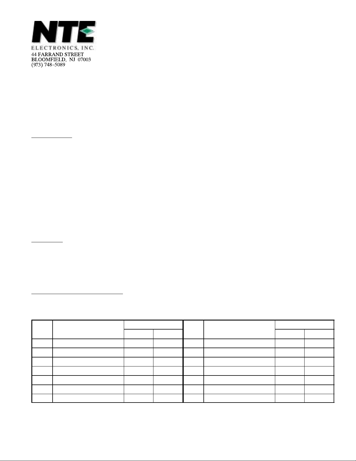
Absolute Maximum Ratings: (TA = +25°C unless otherwise specified)
Operating Ambient Temperature Range, T
Storage Temperature Range, T
stg
opr
–40° to +85°C. . . . . . . . . . . . . . . . . . . . . . . . . . . . . . . . . .
–65° to +150°C. . . . . . . . . . . . . . . . . . . . . . . . . . . . . . . . . . . . . . . . . .
Maximum Voltage and Current Ratings (TA = +25°C) See Table. . . . . . . . . . . . . . . . . . . . . . . . . . . . . . .
Current in mA Current in mA
Pin # Voltage Range in Volts
1 No Connection – – 8 0 to +27 Note 2 1.0
2 No Connection – – 9 0 to +20 1.0 Note 1
3 0 to +5.0 – – 10 No Connection – –
4 0 to +5.0 – – 11 0 to +20 1.0 Note 1
5 No Connection – – 12 No Connection – –
6 0 to +12 – – 13 0 to +20 1.0 Note 1
7 0 to +12 – – 14 Reference 1.0 Note 2
Input Output
Pin # Voltage Range in Volts
Input Output
Note 1. Maximum continuous current output is 20mA and is limited by package power dissipation.
Short circuit current is typically 50mA.
Note 2. Limited by package power dissipation.
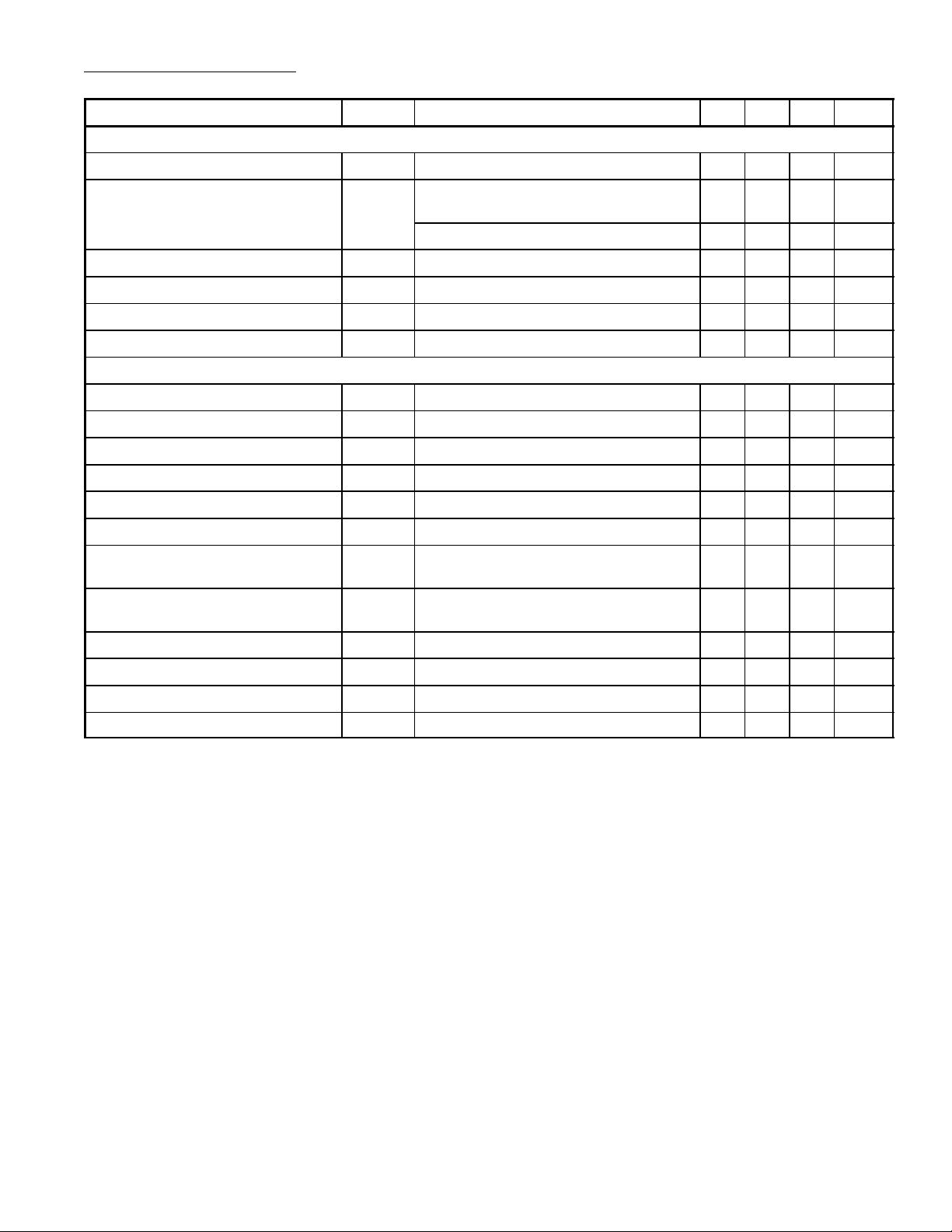
Electrical Characteristics: (TA = +25°C, VCC = 24V, RL = 3.3kΩ, Reference Input Voltage = 1V
P–P
unless otherwise specified)
Parameter T est Pin Test Conditions Min Typ Max Unit
Static Characteristics
Quiescent Output Voltage 9, 11, 13 13.0 14.3 16.0 V
Quiescent Input Current 8 RL = ∞, Chroma and Reference
Voltage = 0
Chroma and Reference Voltage = 0 16.5 19.0 25.5 mA
Reference Input Voltage 6, 7 – 6.6 – V
Chroma Input Voltage 3, 4 – 3.5 – V
Differential Output Voltage 9, 11, 13 Note 3 – 200 600 mV
Output Temperature Coefficient 9, 11, 13 No Output Differential Voltage, Note 3 – 2.0 – mV/°C
Dynamic Characteristics
Detector Output Voltage (B–Y) 13 Note 4 8 13 – V
Chroma Input Voltage 3 B–Y Output = 5V
Detector Output Voltage (G–Y) 9 Adjust B–Y Output to 5V
Detector Output Voltage (R–Y) 11 Adjust B–Y Output to 5V
Relative Output Phase (B–Y to R–Y) 13–11 B–Y Output = 5V
Relative Output Phase (B–Y to G–Y) 13–9 B–Y Output = 5V
Demodulator Unbalanced Voltage 9, 11, 13 No Chroma Input Voltage and Normal
Reference Signal Input Voltage
Residual Carrier and Harmonics 9, 11, 13 With Input Signal Voltage, Normal Refer-
ence Signal Voltage and B–Y = 5V
Reference Input Resistance 6, 7 Chroma Input = 0 – 2.0 – kΩ
, Note 5 – 300 700 mV
P–P
, Note 6 1.4 1.75 2.1 V
P–P
, Note 6 4.3 4.65 5.0 V
P–P
P–P
P–P
P–P
– 6.0 – mA
P–P
P–P
P–P
85 90 95 deg
236 244 252 deg
– 250 500 mV
– – 1.5 V
P–P
P–P
P–P
Reference Input Capacitance 6, 7 Chroma Input = 0 – 6.0 – pF
Chroma Input Resistance 3, 4 – 1.0 – kΩ
Chroma Input Capacitance 3, 4 – 2.0 – pF
Note 3. With chroma input signal voltage = 0 and normal reference input signal voltage (1V
P–P
), all
output voltages will be within specified limits and will not differ from each other by greater
than 0.6V.
Note 4. With normal reference input signal voltage, adjust chroma input signal voltage to 1.2V
P–P
Note 5. With normal reference input signal voltage, adjust chroma input signal voltage until the B–Y
output voltage = 5V
0.7V
P–P
.
. The chroma input voltage at this point should be equal to or less than
P–P
Note 6. With normal reference input signal voltage, adjust the chroma input signal until the B–Y out-
put voltage = 5V
. At this point, the R–Y and G–Y voltages will fall within the specified limits.
P–P
.
 Loading...