

NTE NTE812 Datasheet

NTE812
Integrated Circuit
Audio Power Amplifier, 1W
Description:
The N TE812 i s a m onolithi c i ntegrated c ircuit i n a 1 4–Lead D IP t ype package d esigned f or us e i n d riv er
and power a mpl ifier a pplic ations a t frequencies from 5 0Hz t o 4 0kHz. This device w i ll d el iver u p t o 1 W
RMS o utput p ower i nto a n 8 Ω l oad. The h igh i nput i mpedance a nd l ow s tandby c urrent p rovi de excellent
low–power audio output performance for portable applications. The high peak current capability can
be utilized for direct drivin g of complementary power trans istors in high power amplifier app lica tio ns.
Features:
D 1 Watt RMS Power into 8Ω with THD = 0.65% Typ
D Peak Output Current: 1A
D Wide Supply Voltage Range: 4V to 13V
D High Input Impedance
Applications:
D Radios
D Phonographs
D Portable Communications Receivers
D Complementary Power Amplifier Drivers
D Servo Drivers
Absolute Maximum Ratings: (TA = +25°C unless otherwise specified)
Supply Voltage (Note 1), V
Output Current, I
O
CC
Continuous Power Dissipation (TA ≤ +25°C, Note 2), P
D
15V. . . . . . . . . . . . . . . . . . . . . . . . . . . . . . . . . . . . . . . . . . . . . . . . . . . . . . . .
1A. . . . . . . . . . . . . . . . . . . . . . . . . . . . . . . . . . . . . . . . . . . . . . . . . . . . . . . . . . . . . . . . . . .
1.1W. . . . . . . . . . . . . . . . . . . . . . . . . . . . . . . .
Derate Above 25°C 14.7mW/°C. . . . . . . . . . . . . . . . . . . . . . . . . . . . . . . . . . . . . . . . . . . . . . . . . . . .
Operating Ambient Temperature Range, T
Storage Temperature Range, T
stg
opr
Lead Temperature (During Soldering, 1/16” from case, 10sec), T
L
–55° to +100°C. . . . . . . . . . . . . . . . . . . . . . . . . . . . . . . . .
–65° to +150°C. . . . . . . . . . . . . . . . . . . . . . . . . . . . . . . . . . . . . . . . . .
+260°C. . . . . . . . . . . . . . . . . . . . .
Note 1. Voltage values are with respect to network GND terminal.
Note 2. This rating is valid for the condition that all pins are soldered into a printed circuit board with
a 2” x 2” copper layer area of 14 mil thickness. Most of the heat is conducted to the printed
circuit board copper layer through Pin8 (Input GND).
Electrical Characteristics: (TA = +25°C, VCC = 12V unless otherwise specified)
Parameter Symbol Test Conditions Min Typ Max Unit
Continuous RMS Power Output P
Input Voltage V
THD < 5%, RL = 8Ω, f = 1kHz 1 – – W
O
PO = 1W, RL = 8Ω, f = 1kHz – 45 70 mV
in
Total Harmonic Distortion THD PO = 0.05W RL = 8Ω, f = 1kHz – 0.6 – %
PO = 1W – 0.65 5.0 %
Efficiency PO = 1W, RL = 8Ω, f = 1kHz – 52 – %
Cutoff Frequency
Lower
Reference PO = 1W at 1kHz, RL = 8Ω – 50 – Hz
Upper – 40 – kHz
Input Impedance Z
Output Impedance Z
Reference plane is test
in
circuit input terminal
Reference plane is device output terminal Ω
out
R1 = 100kΩ 80 99 – kΩ
R1 = 2 2kΩ – 22 – kΩ
Noise Output Level (Unfiltered) Reference PO = 1W, Input open – –70 – dB
Quiescent Output Voltage No Signal – 6.2 – V
Quiescent Supply Current No Signal – 5.5 9.0 mA
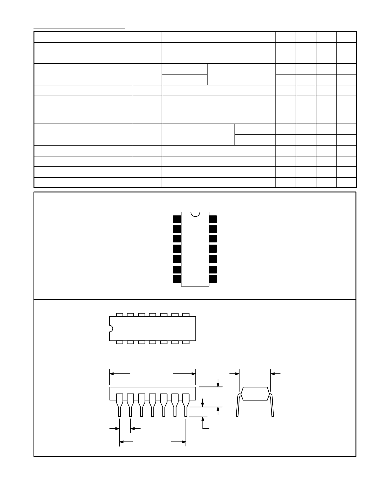
Pin Connection Diagram
Bootstrap
N.C.
Compensation 1
Compensation 2
1
2
3
4
5Feedback
V
14
CC
V
13
CC
12
Output
11
N.C.
10 Output GND
6N.C.
7Input
14 8
17
.785 (19.95)
Max
.100 (2.45) .099 (2.5) Min
.600 (15.24)
9 N.C.
Input GND
8
.200 (5.08)
Max
.300
(7.62)
 Loading...