

NTE NTE788 Datasheet

NTE788
Integrated Circuit
IF System for FM Receiver
Description:
The NTE788 is a monolithic integrated circuit in a 16–Lead DIP type package that provides all the
functions of a comprehensive FM–IF system. This device features a three–stage FM–IF amplifier/limiter configuration with level detectors for each stage, a doubly–balanced quadrature FM detector, and
an audio amplifier that features the optional use of a muting (squelch) circuit.
The advanced circuit design of the IF system includes desirable deluxe features such as delayed AGC
for the RF tuner, an AFC drive circuit, and an output signal to drive a tuning meter and/or provide stereo switching logic. In addition, internal power supply regulators maintain a nearly constant current
drain over the voltage supply range of +8.5V to +16V.
Features:
D Exceptional limiting sensitivity: 12µV typ. at –3dB point
D Low distortion: 0.1% typ. (with double–tuned coil)
D Single–coil tuning capability
D Improved S + N/N Radio
D Externally programmable recovered audio level
D Provides specific signal for control of interchannel muting (squelch)
D On channel step for search control
D Provides programmable AGC voltage for RF amplifier
D Internal supply–voltage regulators
D Externally programmable “ON” channel step width, and deviation at which muting occurs
Absolute Maximum Ratings
: (TA = +25°C unless otherwise specified)
DC Supply Voltage
Between Pin11 and Pin4 16V. . . . . . . . . . . . . . . . . . . . . . . . . . . . . . . . . . . . . . . . . . . . . . . . . . . . . .
Between Pin11 and Pin14 16V. . . . . . . . . . . . . . . . . . . . . . . . . . . . . . . . . . . . . . . . . . . . . . . . . . . . .
DC Current (Out of Pin15) 2mA. . . . . . . . . . . . . . . . . . . . . . . . . . . . . . . . . . . . . . . . . . . . . . . . . . . . . . . . . .
Power Dissipation (Up to T
Derate Above T
Operating Ambient Temperature Range, T
Storage Temperature Range, T
Lead Temperature (During Soldering, 1.32” from case, 10sec max), T
= 85°C), P
A
= +85°C 9.9mW/°C. . . . . . . . . . . . . . . . . . . . . . . . . . . . . . . . . . . . . . . . . . . . . . .
A
stg
D
opr
–65° to +150°C. . . . . . . . . . . . . . . . . . . . . . . . . . . . . . . . . . . . . . . . . .
L
640mW. . . . . . . . . . . . . . . . . . . . . . . . . . . . . . . . . . . . . . . . . .
–40° to +85°C. . . . . . . . . . . . . . . . . . . . . . . . . . . . . . . . . .
+265°C. . . . . . . . . . . . . . . . .
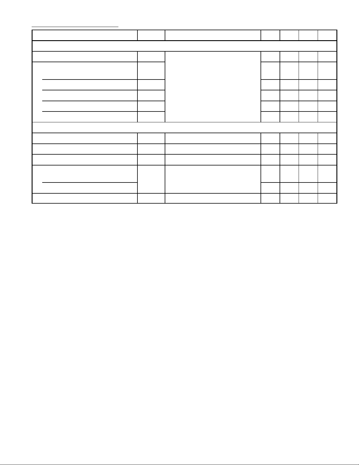
Electrical Characteristics: (TA = +25°C, V+ = 12V unless otherwise specified)
Parameter Symbol Test Conditions Min Typ Max Unit
Static Characteristics
Quiescent Circuit Current I
11
No Signal Input, Non Muted
20 31 40 mA
DC Voltages
IF Input
AC Return to Input V
DC Bias to Input V
RF AGC V
DC Reference V
Dynamic Characteristics (fO = 10.7MHz, f
V
1
2
3
15
10
= 400Hz, Deviation = ±75kHz)
mod
1.2 1.9 2.4 V
1.2 1.9 2.4 V
1.2 1.9 2.4 V
7.5 9.5 11.0 V
5.0 5.6 6.0 V
Input Limiting Voltage V1 (lim) –3dB Point – 12 25 µV
AM Rejection AMR VIN = 0.1V, AM Mod = 30% 45 55 – dB
Recovered AF Voltage VO (AF) VIN = 0.1V 300 400 500 mV
Total Harmonic Distortion
Single Tuned
THD VIN = 0.1V, Note 1 – 0.5 1.0 %
Double Tuned – 0.1 – %
Signal Plus Signal–to–Noise Ratio VIN = 0.1V 60 67 – dB
Note 1. THD characteristics are essentially a function of the phase characteristics of the network
connected between Pin8, Pin9, and Pin10.
 Loading...