

NTE NTE787 Datasheet

NTE787
Integrated Circuit
AM Receiver Subsystem
For Applications in a variety of AM broadcast and communications receivers and applications
requiring an array of amplifiers.
Description:
The NTE787, a monolithic integrated circuit, is an AM subsystem that provides the converter , I F amplifier, detector, and audio preamplifier stages for an AM receiver . It also provides internal AGC for the
first IF amplifier stage, delayed AGC for an optional external RF amplifier, a buffer stage to drive a
tuning meter, and terminals facilitating the optional use of a tone control.
This device features four independent transistor amplifiers, each incorporating internal biasing for
temperature tracking. These amplifiers are particularly useful in general–purpose amplifier, oscillator,
and detector applications in a wide variety of equipment designs.
The NTE787 utilizes a 16–Lead DIP package and operates over an ambient temperature range of
–40° to +85°C.
Features:
D Excellent overload characteristics
D AGC for IF amplifier
D Buffered output signal for tuning meter
D Internal Zener diode provides voltage regulation
D Two IF amplifiers stages
D Low–noise converter and first IF amplifier
D Low harmonic distortion (THD)
D Delayed AGC for RF amplifier
D Terminals for optional inclusion of tone control
D Operates from wide range of power supplies: V+ = 6 to 16 volts
D Optional AC and/or DC feedback on wide–band amplifier
D Array of amplifiers for general–purpose applications
D Suitable for use with optional external RF stage, either MOS or bipolar
Absolute Maximum Ratings: (TA = +25°C unless otherwise specified)
DC Supply Voltage (Across Pin5 and Pin3, Pin6, Pin13, Pin16 respectively) 16V. . . . . . . . . . . . . . .
DC Current
At Pin3, Pin6, Pin13, Pin16 respectively 10mA. . . . . . . . . . . . . . . . . . . . . . . . . . . . . . . . . . . . . . .
At Pin10 30mA. . . . . . . . . . . . . . . . . . . . . . . . . . . . . . . . . . . . . . . . . . . . . . . . . . . . . . . . . . . . . . . . . .
Device Dissipation (Up to T
= +50°C), P
A
D
Derate Above TA = +50°C 7.6mW/°C. . . . . . . . . . . . . . . . . . . . . . . . . . . . . . . . . . . . . . . . . . . . . . .
Operating Ambient Temperature Range, T
Storage Temperature Range, T
stg
opr
Lead Temperature (During Soldering, 1/32” from case, 10sec max), T
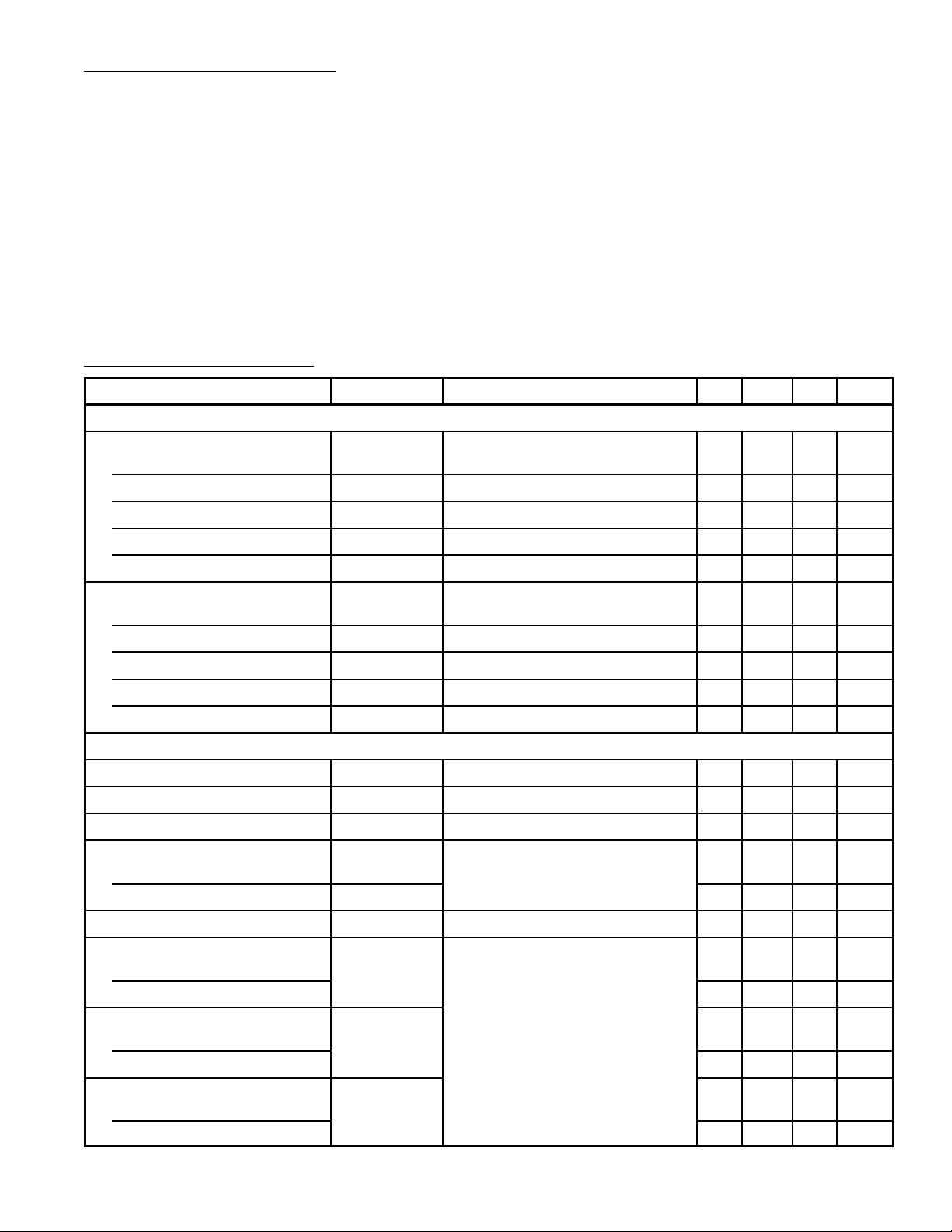
Electrical Characteristics:
Parameter Symbol Test Conditions Min Typ Max Unit
Static Characteristics
DC Voltage
Pin1, Pin4, Pin9, Pin11
Pin2, Pin7, Pin8 V2, V7, V
Pin10 V
Pin12 V
Pin15 V
DC Current
Pin3
Pin6 I
Pin10 I
Pin13 I
Pin16 I
Dynamic Characteristics
(TA = +25°C, V+ = 12V unless otherwise specified)
V1, V4, V9, V
I
10
13
16
11
8
10
12
15
3
6
760mW. . . . . . . . . . . . . . . . . . . . . . . . . . . . . . . . . . . . . . . . .
–40° to +85°C. . . . . . . . . . . . . . . . . . . . . . . . . . . . . . . . . .
–65° to +150°C. . . . . . . . . . . . . . . . . . . . . . . . . . . . . . . . . . . . . . . . . .
L
– 0.7 – V
– 1.4 – V
– 5.6 – V
– 0 – V
– 3.5 – V
– 0.35 – mA
– 1.0 – mA
– 20 – mA
– 0 – mA
– 1.2 – mA
+265°C. . . . . . . . . . . . . . . . .
Detector Output 30% Modulation – 75 – mV
Audio Amplifier Gain A
AF
Audio Distortion V
f = 1kHz – 30 – dB
= 100mV – 0.2 – %
OUT
Sensitivity
At Converter Stage Input
At RF Stage Input
fIN = 1MHz,
Signal–to–Noise Ratio (S/N) = 20dB
– 200 – µV/m
– 100 – µV/m
Total Harmonic Distortion THD 30% Modulation – 1.0 – %
Input Resistance
At Transistor Q1
At Transistor Q5
R
IN
No AGC,
Input Frequency Signal (fIN) = 1MHz
– 3500 – Ω
– 2000 – Ω
Input Capacitance
At Transistor Q1
C
IN
– 17 – pF
At Transistor Q5 – 12 – pF
Feedback Capacitance
At Transistor Q1
C
FB
– 1.5 – pF
At Transistor Q5 – 1.5 – pF
rms
 Loading...