

NTE NTE778A, NTE778SM Datasheet
NTE778A & NTE778SM
Integrated Circuit
Dual Operational Amplifier
Description:
The NTE778A (8–Lead DIP) and NTE778SM (SOIC–8 Surface Mount) are linear integrated circuits
designed for use as a summing amplifier, integrator, or amplifier with operating characteristics as a
function of the external feedback components.
Features:
D No Frequency Compensation Required
D Short–Circuit Protection
D Wide Common–Mode and Differential Voltage Ranges
D Low Power Consumption
D No Latch Up
Absolute Maximum Ratings:
Power Supply Voltage, V
Input Differential Voltage, V
Input Common Mode Voltage (Note 1), V
Output Short–Circuit Duration (Note 2), t
Operating Junction Temperature, T
Operating Ambient Temperatue Range, T
Storage Temperature Range, T
(TA = +25°C unless otherwise specified)
, V
CC
EE
ID
ICM
S
J
A
stg
±18V. . . . . . . . . . . . . . . . . . . . . . . . . . . . . . . . . . . . . . . . . . . . . . . . . . . .
±30V. . . . . . . . . . . . . . . . . . . . . . . . . . . . . . . . . . . . . . . . . . . . . . . . . . . . . . .
±15V. . . . . . . . . . . . . . . . . . . . . . . . . . . . . . . . . . . . . . . . . .
Continuous. . . . . . . . . . . . . . . . . . . . . . . . . . . . . . . . . . . . . .
+150°C. . . . . . . . . . . . . . . . . . . . . . . . . . . . . . . . . . . . . . . . . . . . . . .
0° to +70°C. . . . . . . . . . . . . . . . . . . . . . . . . . . . . . . . . . . . .
–55° to +125°C. . . . . . . . . . . . . . . . . . . . . . . . . . . . . . . . . . . . . . . . . .
Note 1. For s upply v oltages l ess t han ±15V , t he a bsolute m aximum input voltage i s e qual t o t he s upply
voltage.
Note 2. Supply voltage equal to or less than ±15V.
Electrical Characteristics:
Parameter Symbol Test Conditions Min Typ Max Unit
Input Offset Voltage V
Input Offset Current I
Input Bias Current I
(TA = 0° to +70°C, VCC = +15V, VEE = –15V unless otherwise specified)
RS ≤ 10kΩ – – 7.5 V
IO
RS ≤ 10kΩ, TA = +25°C – 2.0 6.0 V
IO
TA = +25°C – 20 200 nA
IB
TA = +25°C – 80 500 nA
– – 300 nA
– – 800 nA
Electrical Characteristics (Cont’d): (TA = 0° to +70°C, VCC = +15V, VEE = –15V unless otherwise
specified)
Parameter Symbol Test Conditions Min Typ Max Unit
Input Capacitance C
Common–Mode Input Voltage Range V
Large Signal Voltage Gain A
Output Resistance t
Common–Mode Rejection Ratio CMRR RS ≤ 10kΩ, TA = +25°C 70 90 – dB
Supply Voltage Rejection Ratio PSRR RS ≤ 10kΩ, TA = +25°C – 30 150 µV/V
Output Voltage Swing V
Output Short–Circuit Current I
Supply Currents (Both Amplifiers) I
Power Consumption (Both Amplifiers) P
Transient Response (Unity Gain, TA = +25°C)
Rise Time t
Overshoot os – 15 – %
ICR
os
TLH
TA = +25°C – 1.4 – pF
i
TA = +25°C ±12 ±13 – V
VO = ±10V, RL = 2kΩ 15 – – V/mV
V
VO = ±10V, RL = 2kΩ, TA = +25°C 20 200 – V/mV
TA = +25°C – 75 – Ω
o
RS ≥ 10kΩ ±12 ±14 – V
O
RS ≥ 10kΩ, TA = +25°C ±12 ±14 – V
RS ≥ 2kΩ ±10 ±13 – V
RS ≥ 2kΩ, TA = +25°C ±10 ±13 – V
TA = +25°C 10 20 40 mA
TA = +25°C – 2.3 5.6 mA
D
TA = +25°C – 70 170 mW
C
VI = 20mV, RL ≥ 2kΩ, CL ≤ 100pF – 0.3 – µs
Slew Rate
NTE778A
NTE778SM 1.0 1.6 – V/µs
Output 1
Invert Input 1
Non–Invert Input 1
SR VI = 10V, RL ≥ 2kΩ, CL ≤ 100pF – 0.5 – V/µs
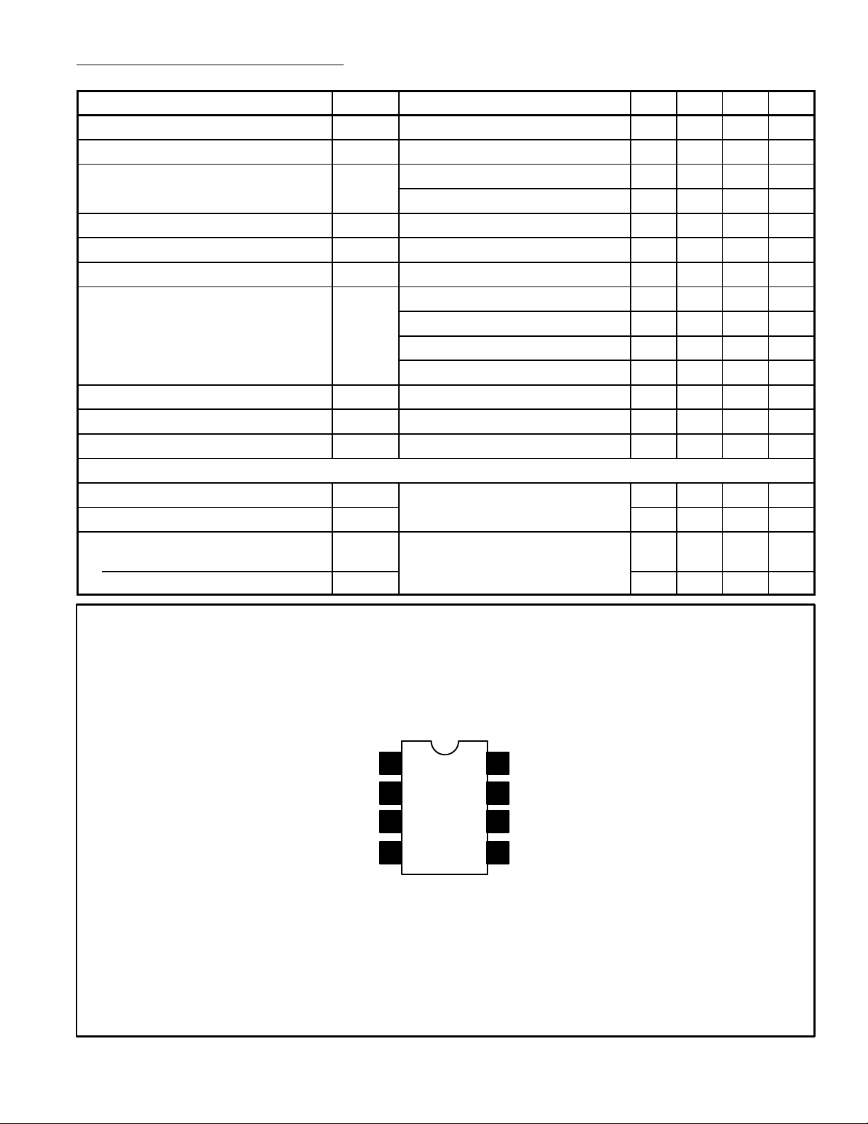
Pin Connection Diagram
V (–)
1
2
3
4
8
V (+)
Output 2
7
Invert Input 2
6
5
Non–Invert Input 2
 Loading...