

NTE NTE747 Datasheet

NTE747
Integrated Circuit
Low Level Video Detector
Description:
The NTE747 is a low level video detector in an 8–Lead DIP type package featuring very linear video
characteristics and bandwidth. Designed for color and monochrome television receivers, replacing
the third IF, detector, video buffer, and the AFC buffer.
Features:
D Conversion Gain: 34dB Typ
D Video Frequency Response @ 6MHz < 1dB
D Input of 36mV Produces 3V
D High Video Output: 7.7V
P–P
D Fully Balanced Detector
D High Rejection of IF Carrier
D Low Radiation of Spurious Frequencies
P–P
Output
Absolute Maximum Ratings:
(TA = +25°C unless otherwise specified)
Power Supply Voltage 24V. . . . . . . . . . . . . . . . . . . . . . . . . . . . . . . . . . . . . . . . . . . . . . . . . . . . . . . . . . . . . .
Supply Current 26mA. . . . . . . . . . . . . . . . . . . . . . . . . . . . . . . . . . . . . . . . . . . . . . . . . . . . . . . . . . . . . . . . . . .
Input Voltage 1V
. . . . . . . . . . . . . . . . . . . . . . . . . . . . . . . . . . . . . . . . . . . . . . . . . . . . . . . . . . . . . . . . . . .
Power Dissipation 625mW. . . . . . . . . . . . . . . . . . . . . . . . . . . . . . . . . . . . . . . . . . . . . . . . . . . . . . . . . . . . . .
Derate Above 25°C 5mW/°C. . . . . . . . . . . . . . . . . . . . . . . . . . . . . . . . . . . . . . . . . . . . . . . . . . . . . . .
Operating Ambient Temperature Range 0° to +75°C. . . . . . . . . . . . . . . . . . . . . . . . . . . . . . . . . . . . . . . .
Storage Temperature Range –65° to +150°C. . . . . . . . . . . . . . . . . . . . . . . . . . . . . . . . . . . . . . . . . . . . . . .
Electrical Characteristics:
Parameter Pin Test Conditions Min Typ Max Unit
Supply Voltage Range 6 12 20 24 V
Supply Current 5, 6 – 15 – mA
Zero Signal DC Output Voltage 4 6.8 7.7 8.3 V
Maximum Signal DC Output Voltage 4 – 0 – V
Input Signal Voltage 7 3V
(TA = +25°C, V+ = 20V, Q = 30, fC = 45MHz unless otherwise specified)
Video Output, 90% Modulation – 36 – mV
P–P
RMS
RMS
Electrical Characteristics: (TA = +25°C, V+ = 20V, Q = 30, fC = 45MHz unless otherwise specified)
Parameter Pin Test Conditions Min Typ Max Unit
Maximum Output Voltage Swing 4 – 7.7 – V
Carrier Rejection at Output 4 42 60 – dB
Carrier Output Voltage 3V
3V
Output, f
P–P
Output, f
P–P
out
out
= f
= 2f
C
C
– 1 – mV
– 3 – mV
3dB bandwidth of IF carrier 7 – 80 – MHz
3dB Bandwidth of Video Output 4 – 12.3 – MHz
Input Resistance 7 – 3.5 – kΩ
Input Capacitance 7 – 3.0 – pF
Internal Resistance 2, 3 Across Tuned Circuit – 4.4 – kΩ
Internal Capacitance 2, 3 – 1.0 – pF
AFT Buffer Output 1 At Carrier Frequency, Note 1 – 350 – mV
AFT Buffer DC Level 1 – 6.5 – V
Note 1. Measured with 10 times probe.
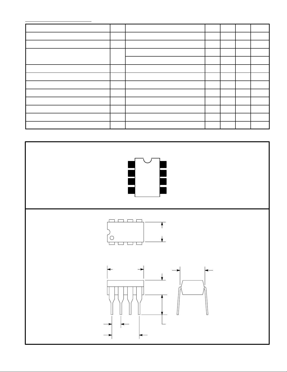
Pin Connection Diagram
AFT Buffer
1
GND
8
P–P
P–P
P–P
P–P
Tuned Circuit
Tuned Circuit
Primary Video Output
85
14
.390 (9.9)
Max
2
3
4
IF Input
7
V
6
CC
5
Aux Video Output
.260 (6.6)
.155
(3.93)
.300
(7.62)
.100 (2.54)
.145 (3.68)
.300 (7.62)
 Loading...