

NTE NTE744 Datasheet

NTE744
Integrated Circuit
RF/IF Amp
Description:
The NTE744 is a monolithic silicon integrated circuit that provides an rf amplifier, if amplifier, mixer,
oscillator, AGC detector, and voltage regulator on a single chip. It is intended for use in super–heterodyne AM radio receiver applications particularly in automobiles. The NTE744 is supplied in a 14–lead
dual–in–line plastic package and operates over the temperature range of –55° to 125°C.
Features:
D Low–noise, low–Rb, rf stage in cascode connection–eliminates Miller–Effect regeneration and
allows controlled power rise by the choice of external components.
D Mixer–oscillator stage with internal feedback–eliminates need for tapped or multi–winding os-
cillator coils
D Cascode if amplifier with controlled output impedance and negligible Miller Effect–eliminates
regeneration and selectivity skewing
D Frequency–counter AGC circuit–allows control of AGC response by selection of the coupling
capacitor.
D Integral regulation with built–in surge protection
D Separately accessible amplifiers
Absolute Maximum Ratings:
DC Supply Voltage (Pin3), V+ 9V. . . . . . . . . . . . . . . . . . . . . . . . . . . . . . . . . . . . . . . . . . . . . . . . . . . . . . . . .
DC Supply Voltage (IF Output, Pin6) 40V. . . . . . . . . . . . . . . . . . . . . . . . . . . . . . . . . . . . . . . . . . . . . . . . . .
DC Supply Voltage (RF Output, Pin13) 20V. . . . . . . . . . . . . . . . . . . . . . . . . . . . . . . . . . . . . . . . . . . . . . . .
DC Supply Voltage (Mixer Output, Pin14) 20V. . . . . . . . . . . . . . . . . . . . . . . . . . . . . . . . . . . . . . . . . . . . . .
DC Current (Pin3) 35mA. . . . . . . . . . . . . . . . . . . . . . . . . . . . . . . . . . . . . . . . . . . . . . . . . . . . . . . . . . . . . . . .
Power Dissipation (Up to T
Derate Above T
Operating Ambient Temperature Range, T
Storage Temperatur Range, T
Lead Temperature (During Soldering, 1/16” (1.59mm)from case, 10sec max), T
= +55°C), P
A
= 55°C 6.67mW/°C. . . . . . . . . . . . . . . . . . . . . . . . . . . . . . . . . . . . . . . . . . . . . . .
A
stg
D
opr
L
750mW. . . . . . . . . . . . . . . . . . . . . . . . . . . . . . . . . . . . . . . . .
–55° to +125°C. . . . . . . . . . . . . . . . . . . . . . . . . . . . . . . . .
–65° to +150°C. . . . . . . . . . . . . . . . . . . . . . . . . . . . . . . . . . . . . . . . . . . .
+265°C. . . . . . . .
Electrical Characteristics: (TA = +25°C unless otherwise specified)
Parameter Symbol Test Conditions Min Typ Max Unit
Static Characteristics
DC Voltage
At Pin1, Pin4
At Pin2, Pin3, Pin14 V2, V3, V
At Pin5 V
At Pin6 V
At Pin7 V
At Pin8, Pin9 V8, V
At Pin10, Pin11 V10, V
At Pin12 V
At Pin13 V
DC Current
Into Pin1, Pin4, Pin5, Pin7,
Pin8, Pin9, Pin10, Pin11, Pin12
Into Pin2 I
Into Pin3 I
Into Pin6 I
Into Pin13 I
Into Pin14 I
Performance Characteristics
V1, V
5
6
7
12
13
I1, I4, I5, I7,
I
, I9, I10, I
8
2
3
6
13
14
4
14
9
11
12
– 4.7 – V
– 6.8 – V
– 0.25 – V
– 12 – V
– 0.76 – V
– 0 – V
– 0.71 – V
– 0.71 – V
– 4.0 – V
– 0 – mA
– 1.2 – mA
– 15 – mA
– 4.3 – mA
– 4.5 – mA
– 0.17 – mA
Sensitivity Input Signal to Dummy Antenna at
f
= 1MHz, 30% AM Modulation at
IN
f
= 400Hz, for 11mV Output at V
MOD
O
Signal–to–Noise Ratio S/N Ratio of Output at VO with Modulation
ON & the OFF, Input Signal = 100µV,
30% AM Modulation at f
MOD
= 400Hz
Overload Distortion Input Signal set at 1MHz, 90% AM
Modulation, Distortion at V
must be
O
≤ 10%
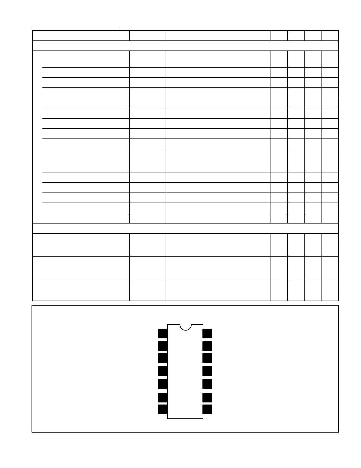
Pin Connection Diagram
Mixer Input
OSC Tank
V
CC
Mixer Bypass
1
2
3
4
5AGC Drive
6IF Output
14
Mixer Output
RF Output
13
RF Input
12
11
RF Bypass
10 AGC Capacitor
9 RF GND
– 2.3 – µV
34 43 – dB
160k 400k – µV
7IF Input
Substrate & IF Amp GND
8
 Loading...