

NTE NTE740A Datasheet
NTE740A
Integrated Circuit
Audio Power Amp, 2W
Description:
TheNTE740A i s a n A udio P ower A mplifi er in a 1 4–Lead DIP t ype p ackage d esi gned for m ini mal e xternal
component requirements.
Features:
D Low Distortion
D Low Quiescent Current
D 34dB Internally Fixed Gain
D High Input Impedance
D Thermal Overload Protection
D Output Short Circuit Current Limiting
Absolute Maximum Ratings:
Supply Voltage, V
Peak Output Current, I
Operating Ambient Temperature Range, T
Storage Temperature Range, T
CC
O
A
stg
–25° to +70°C. . . . . . . . . . . . . . . . . . . . . . . . . . . . . . . . . . .
–65° to +150°C. . . . . . . . . . . . . . . . . . . . . . . . . . . . . . . . . . . . . . . . . .
Electrical Characteristics: (TA = +25°C, VCC = 18V, f = 1kHz, RL = 8Ω unless otherwise specified)
Parameter Symbol Test Conditions Min Typ Max Unit
Supply Voltage Range V
Quiescent Supply Current I
Quiescent Output Voltage V
Output Voltage Swing V
Voltage Gain A
Total Harmonic Distortion THD P
Audio Output Power P
Input Impedance Z
Power Supply Rejection Ratio PSRR P
Equivalent Input Noise Voltage f = 20Hz to 20kHz – 60 – µV
Sensitivity Input Voltage e
Bandwidth (–3dB) BW P
CC
CC
OQ
out
No Signal Applied – 15 – mA
No Signal Applied, Note 1 9 – – V
P
O
V
in
in
= 2W – 12 – V
out
P
= 0 31 34 37 dB
out
= 2W, Note 2 – 1.0 2.0 %
out
P
= 50mW, Note 3 – 0.5 1.0 %
out
THD = 2%, RL = 8Ω, Note 4 2.0 2.5 – W
THD = 2%, RL = 16Ω, Note 4 2.0 2.5 – W
Each Input 140 170 – kΩ
= 0, f = 120Hz, Note 5 – 40 – dB
out
e
= 4.0V
out
= 1W, Note 6 – 100 – kHz
out
rms
, P
= 2W – 80 – mV
out
9 10 26 V
26V. . . . . . . . . . . . . . . . . . . . . . . . . . . . . . . . . . . . . . . . . . . . . . . . . . . . . . . . . . . . . . . .
1.2A. . . . . . . . . . . . . . . . . . . . . . . . . . . . . . . . . . . . . . . . . . . . . . . . . . . . . . . . . . . .
P–P
rms
Note 1. The quiescent output voltage typically equals 1/2 the normal VCC voltage = 1 Volt.
Note 2. When driving a 16Ω load, the nominal VCC is 24V.
Note 3. When driving a 16Ω load, the maximum low level distortion is reduced to 0.50%.
Note 4. Tested at VCC equals nominal and measured in watts (rms).
Note 5. Measurement made with a 5µF capacitor from Pin1 to GND. Voltage at Pin14 is at a ripple
frequency of 60Hz.
Note 6. Unity gain occurs between 10 and 100MHz.
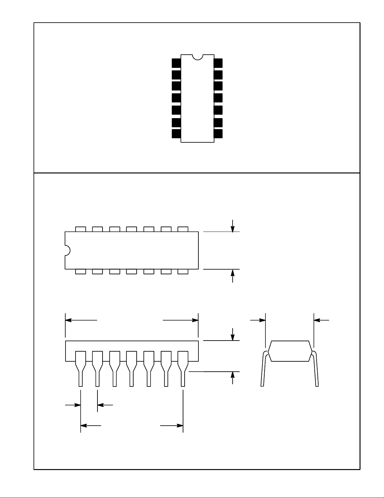
Pin Connection Diagram
Bypass
(+) Input
GND
GND
1
2
3
4
5GND
6(–) Input
7GND
14 8
V
14
CC
N.C.
13
GND
12
11
GND
10 GND
9 N.C.
Output
8
.280 (7.1)
Max
17
.770 (19.5) Max
.300 (7.62)
.160 (4.0)
Max
.100 (2.45)
.600 (15.24)
 Loading...