

NTE NTE726 Datasheet
NTE726
Integrated Circuit
Wide Band Amplifier
Features:
D Exceptionally High Amplifier Gain: Power Gain at 4.5MHz/s – 75dB (Typ)
D Excellent Limiting Characteristics: Input Limiting Voltage (Knee) = 600µV (Typ) at 10.7MHz/s
D Wide Frequency Capability: 100kHz/s to > 20MHz/s
Absolute Maximum Ratings:
Recommended Minimum DC Supply Voltage, V
(TA = +25°C unless otherwise specified)
CC
Minimum Input Signal Voltage (Between Pin1 and Pin2) ±3V. . . . . . . . . . . . . . . . . . . . . . . . . . . . . . . . .
Maximum Device Dissipation, P
Operating Temperature Range, T
Storage Temperature Range, T
Lead Temperature (During Soldering, 1/16” from case, 10sec max), T
Electrical Characteristics:
Parameter Symbol Test Conditions Min Typ Max Unit
Total Device Dissipation P
Voltage Gain A VCC = 6V, f = 1Mc/s, Note 2 60 66 – dB
Input–Impedance Components
Parallel Input Resistance R
Parallel Input Capacitance C
Output–Impedance Components
Parallel Output Resistance R
Parallel Output Capacitance C
Noise Figure NF VCC = 7.5V, f = 4.5Mc/s – 8.7 – dB
Input Limiting Voltage (Knee) v
D
opr
stg
(TA = +25°C unless otherwise specified)
VCC = 6V, Note 1 66 90 121 mW
T
VCC = 7.5V, Note 1 97 120 167 mW
VCC = 10V, Note 1 150 190 255 mW
VCC = 7.5V, f = 1Mc/s, Note 2 65 70 – dB
VCC = 7.5V, f = 4.5Mc/s, Note 2 60 67 – dB
VCC = 7.5V, f = 10.7Mc/s, Note 2 55 61 – dB
VCC = 10V, f = 1Mc/s, Note 2 65 71 – dB
VCC = 7.5V, f = 4.5Mc/s – 3 – kΩ
IN
IN
OUT
OUT
i(lim)
VCC = 7.5V, f = 4.5Mc/s – 31.5 – kΩ
VCC = 7.5V, f = 4.5Mc/s – 300 400 µV
–55° to +125°C. . . . . . . . . . . . . . . . . . . . . . . . . . . . . . . . . . . . . . . .
–65° to +150°C. . . . . . . . . . . . . . . . . . . . . . . . . . . . . . . . . . . . . . . . . .
L
– 7 – pF
– 4.2 – pF
300mW. . . . . . . . . . . . . . . . . . . . . . . . . . . . . . . . . . . . . . . . . . . . . . . . .
+265°C. . . . . . . . . . . . . . . . .
5.5V. . . . . . . . . . . . . . . . . . . . . . . . . . . . . . . . . . . . .
Note 1. The total current drain may be determined by dividing PT by VCC.
Note 2. Recommended minimum DC supply voltage (V
) is 5.5V. Nominal load current flowing into
CC
Pin5 is 1.5mA at 7.5V.
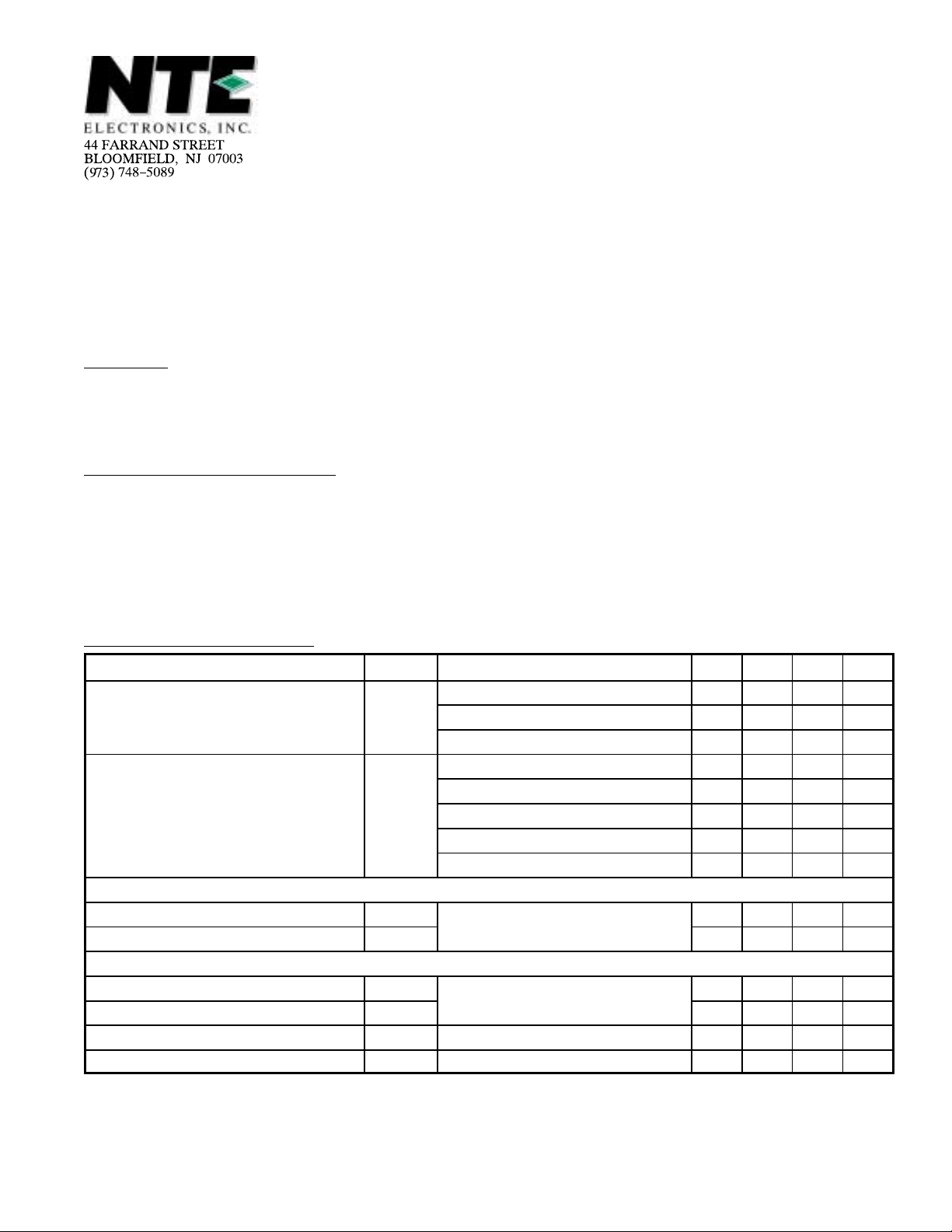
Pin Connection Diagram
(Top View)
Internal Connection* Internal Connection*
GND
Internal Connection*
*NOTE: These leads are internally connected. DO NOT USE.
8
9
10
V
CC
IF Input High
7
1
6
IF Output
5
4
3
Bypass
2
IF Input Reference
.335 (8.52) Dia Max
.175
(4.45)
Max
Bypass
.500
(12.7)
Min
.018 (0.45) Dia Typ
.100 (2.54)
3
2
4
5
.370
1
6
(9.4)
Max
7
10
9
8
.200 (5.08) Dia
 Loading...